AllenĆBradley Absolute Encoder Module (Cat. No.
Table of Contents Using This Manual . . . . . . . . . . . . . . . . . . . . . . . . . . . . . . . 1Ć1 Chapter Objectives . . . . . . . . . . . . . . . . . . . . . . . . . . . . . . . . . . . What This Manual Contains . . . . . . . . . . . . . . . . . . . . . . . . . . . . Audience . . . . . . . . . . . . . . . . . . . . . . . . . . . . . . . . . . . . . . . . . . Warnings and Cautions . . . . . . . . . . . . . . . . . . . . . . . . . . . . . . . Summary . . . . . . . . . . . . . . . . . . . . . . . . . .
ii Table of Contents Offset Feature . . . . . . . . . . . . . . . . . . . . . . . . . . . . . . . . . . 5Ć1 Offset Feature . . . . . . . . . . . . . . . . . . . . . . . . . . . . . . . . . . . . . . Offset Words . . . . . . . . . . . . . . . . . . . . . . . . . . . . . . . . . . . . . . . Programming Considerations with Offset . . . . . . . . . . . . . . . . . . . 5Ć1 5Ć2 5Ć6 Troubleshooting . . . . . . . . . . . . . . . . . . . . . . . . . . . . . . . . 6Ć1 Chapter Objectives . . . . . . . . . . .
Chapter 1 Using This Manual Chapter Objectives Read this chapter to familiarize yourself with this manual. It tells you how to use the manual properly and efficiently.
Chapter 1 Using This Manual If you do not know how to do either of these, read the user’s manual of your processor. Refer to our Publications Index (publication SD499) for a complete list of publications. Warnings and Cautions Throughout this manual we include special notes to alert you to possible injury to personnel or damage to equipment under specific circumstances. WARNING: tells you when people may be injured if procedures are not followed properly.
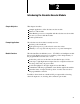
Chapter 2 Introducing the Absolute Encoder Module Chapter Objectives This chapter describes: example applications of the absolute encoder module functions of the module Allen-Bradley processors compatible with the absolute encoder module encoders you can use with the module module specifications Example Applications The absolute encoder module is usually used for: absolute-position feedback high-speed response to position based on encoder values immunity to loss of position from power loss or power in
Chapter 2 Introducing the Absolute Encoder Module Compatible Processors You can use the absolute encoder module with any Allen-Bradley programmable controller that uses block-transfer programming in both local and remote 1771 I/O systems. Processors that are compatible with the module include: Mini PLC-2 (cat. no. 1772-LN3) PLC-2/20 (cat. no. 1772-LP1, -LP2) PLC-2/30 (cat. no. 1772-LP3) PLC-3 (cat. no. 1775-L1, -L2) Mini-PLC-2/15 (cat. no. 1772-LV) Mini-PLC-2/05 (cat. no.
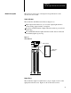
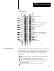
Chapter 2 Introducing the Absolute Encoder Module Module Description The next four sections give a description and specifications of the absolute encoder module. Status Indicators The module has 10 LED status indicators (Figure 2.1): Eight output status indicators (one for each output) light when the corresponding output circuitry is energized. One green ACTIVE indicator lights when the module is powered and functioning.
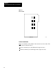
Chapter 2 Introducing the Absolute Encoder Module Figure 2.2 Fuse Locations F1 F2 F3 F4 F5 F6 F7 F8 Right Board 13303 Terminal Identification Figure 2.3 identifies each terminal of the absolute encoder module.
Chapter 2 Introducing the Absolute Encoder Module Figure 2.
Chapter 2 Introducing the Absolute Encoder Module CAUTION: Electrostatic discharge can degrade performance or damage the module. Handle as stated above. Specifications 2Ć6 Module Location Any 1771ĆI/O chassis; any 2Ćslot I.O group Input Power Supply +5V DC +0.
Chapter 2 Introducing the Absolute Encoder Module New Position Throughput Time 200 us Environmental Conditions Operating Temperature 0 to 60o C (32 to 140oF) Storage Temperature Ć40 to 85oC (Ć40 to 185oF) Relative Humidity 5 to 95% (without condensation) New WriteĆdata Throughput Time 4.
Chapter 3 Configuring and Installing Your Module Chapter Objectives This chapter tells you how to: select module features by setting configuration plugs power module input circuitry and output devices key the module make wiring arm connections install the module Electrostatic Discharge Electrostatic discharge can damage integrated dircuits or semiconductors in this module if you touch backplane connector pins.
Chapter 3 Configuring and Installing Your Module Figure 3.
Chapter 3 Configuring and Installing Your Module Figure 3.2 Configuration Plug Location and Settings (Right Board) E1 Down Right Board Configuration Configuration Plug Settings Plug State of Outputs After Loss of Input Power Supply E1 Turn Off Last State Up Down 13305 Selecting Encoder Format and Input Signal Mode Set configuration plugs E1 through E12 (on the left board) to match the signal mode of each encoder input channel to the encoder.
Chapter 3 Configuring and Installing Your Module encoders. This is the same as selecting “high true” or “low true” inputs from the Gray encoder. Configuration plug E15 is factory-set in the right position. It gives an increased count when the encoder rotates clockwise when looking at the shaft. If your encoder shows a decreased count, change the plug to the left position.
Chapter 3 Configuring and Installing Your Module I/O chassis module slot. They also help to align the module with the backplane connector. Each module is slotted at its rear edge. The position of the keying bands must correspond to these slots to allow insertion of the module. Position the keying bands on the upper backplane connector between the numbers at the right of the connectors. Keying bands are only used to key slot 0 of the module. Figure 3.
Chapter 3 Configuring and Installing Your Module maximum of 300mA. For the best system noise immunity, we recommend use of a separate, linear regulated power supply for powering the input circuitry and the encoder. You can use this supply for more than one absolute encoder module or encoder, but do not use it for otehr 5V loads such as relays. Make sure the power supply has enough additional current capacity for the encoder.
Chapter 3 Configuring and Installing Your Module Output Power Supply To power the eight outputs (Figure 3.5), connect at least one +5 to +24V DC supply to terminal 1 and terminal 6 (or 7) of the right wiring arm. You can connect another +5 to +24V DC power supply between terminals 9 and 14 (or 15) of the right wiring arm if, for example, you need two different load supply voltages.
Chapter 3 Configuring and Installing Your Module WiringĆArm Connections We recommend the following Belden cable or its equivalent to connect the encoder to the module (maximum 50 feet). Use extra twisted pairs to connect power to the encoder. No. of No. of Twisted Belden Cable No. Encoder Bits Pairs in Cable 18 AWG 20 AWG 8 9 9775 9875 10 11 Ć 9876 Ć 12 9776 9877 12 15 9777 9879 Important: Tighten wiring arm connections to 9 inch-pounds of torque.
Chapter 3 Configuring and Installing Your Module Figure 3.6 SingleĆended Output Encoder Connection Diagram Left Wiring Arm Single-ended Ouput Encoder Bit 0 Common Bit 1 Common Bit 2 Common Power Supply Common Other bit connections not shown. Continue in this manner until you make all bit connections. If the encoder uses less than 12 bits, jumper the unused input terminals.
Chapter 3 Configuring and Installing Your Module Figure 3.7 Differential Output Encoder Connection Diagram Left Wiring Arm Differential Ouput Encoder Bit 0 Bit 0 Bit 1 Bit 1 Bit 2 Bit 2 Other bit connections not shown. Continue in this manner until you make all bit connections. If the encoder uses less than 12 bits, jumper the unused input terminals.
Chapter 3 Configuring and Installing Your Module Installing the Module Now that you’ve determined the power requirements, keying, and wiring for your module, you can use the following procedure to install it. Refer to the Programmable Controller Grounding and Wiring Guidelines (pub. no. 1770-4.1) for proper grounding and wiring methods to install your module. WARNING: Remove power from the 1771 I/O chassis backplane and wiring arm before installing or removing the module.
Chapter 3 Configuring and Installing Your Module Summary 3Ć12 This chapter told you how to select features and set configuration plugs on the absolute encoder module, and described the power requirements, keying, wiring, and installation of the module. In the next chapter you will read about block-transfer file parameters.
Chapter 4 Module/Processor Communication Chapter Objectives This chapter describes file parameters for the block-transfer data files you use to write data to and read data from the absolute encoder module. Block Transfer The absolute encoder module and the processor communicate through block-transfer programming. Processors that use block-transfer programming are listed below, along with the respective programming manual.
Chapter 4 Module/Processor Communication outputs 4 and 5 (and the module is controlling all eight outputs), you must send 20 words to the module; you cannot send only the words associated with outputs 4 and 5. Figure 4.
Chapter 4 Module/Processor Communication Control Words Each control word is associated with two outputs. The lower byte of control word 1 is associated with output 0. Its format is as follows: Bits 0 through 2 are the comparison bits for output 0, preset A (greater than, less than, equal to, greater than or equal to, less than or equal to). Bits 3 through 5 are the comparison bits for output 0, preset B. Bit 6 is the zero transition (ZT) bit.
Chapter 4 Module/Processor Communication WriteĆData Throughput Time Thewrite-data throughput time is the time between the end of a block-transfer-write operation and the module update of its outputs. The module’s response time can vary, depending on the number of outputs it controls, the type of absolute encoder you use, and if you have an offset value. The worst case is 4.7 ms. Use the following table to determine the module’s response time in milliseconds for your application.
Chapter 4 Module/Processor Communication Bit 7 is the loss-of-input-power bit. It is set when input power is lost; it is reset when power is restored and bit 6 is reset. Bit 6 is the write-data-valid bit. It is set at power-up and when the processor changes from the program mode to the run mode; it is reset when the module receives valid data in a block-transfer-write operation. Bit 5 is unused. Bit 4 is the non-BCD preset flag. It is set when any preset is in non-BCD format.
Chapter 4 Module/Processor Communication the OE bit Output 0 is turned on when the shaft position is greater than or equal to 330 or when the shaft position is less than or equal to 005. If you don’t set the ZT bit in the above control word, when the encoder shaft position is 002, for example, comparison B is true, comparison A is not true, and the output is turned off. (At position 002, the shaft position is less than or equal to 005, but it is not greater than or equal to 330.
Chapter 4 Module/Processor Communication Programming Considerations When you specify the default block length (00), the following considerations apply for PLC-2 family processors: You can and should enable the read and write instructions in the same scan (separate but equal input conditions). The module decides which operation is performed first when both instructions are enabled in the same scan. Alternate operation is performed in a subsequent scan.
Chapter 5 Offset Feature Offset Feature Offset is a new feature of the Absolute Encoder Module (cat. no. 1771-DE, revision B). Revision A modules do not have this feature. Offset is the difference between the 0 position of the absolute encoder and the 0 position of the machine shaft to which the encoder is connected. You can program this value to compensate for such factors as machine wear or improper mechanical setup.
Chapter 5 Offset Programming In this example, the 0 machine position is “ahead” of the 0 encoder position. Depending on which equation you use (your reference point), the offset value is either positive or negative. Offset Value From 0 Encoder Position and From 0 Machine Position 0 3584 Encoder 0 512 Machine shaft At encoder position 0, machine shaft position is 512. The offset is +3,584. At machine shaft position 0, encoder position is 3,584. The offset is Ć512.
Chapter 5 Offset Programming Format of Offset Words 17 16 15 14 13 12 S 11 10 7 6 5 4 3 2 1 0 Bit # OFFSET VALUE NO. OF ENCODER POSITIONS The offset words are the last two words of the write-data block that you send to the absolute encoder module. If you are controlling 2 outputs 4 outputs 6 outputs 8 outputs The offset words are: words 6 and 7 words 11 and 12 words 16 and 17 words 21 and 22 S = sign bit.
Chapter 5 Offset Programming Figure 5.1 Format of BlockĆtransferĆwrite Data with Offset 17 16 15 14 13 12 11 10 07 06 05 04 03 02 01 00 Word #1 OE ZT > = < > = < OE ZT > = < > = < 2 3 Preset 0B 4 Preset 1A 5 Preset 1B Control Word for Outputs 2 and 3 Preset 2A 6 OE ZT > 7 A.
Chapter 5 Offset Programming Bit 7 is the loss-of-input-power bit. It is set when input power is lost; it is reset when power is restored and bit 6 is reset. Bit 6 is the write-data-valid bit. It is set at power-up and when the processor changes from program mode to run mode; it is reset when the module receives valid data in a block-transfer-write operation. Bit 5 is the non-BCD offset flag. See the description of bit 0 and bit 1 below to identify the type of offset error.
Chapter 5 Offset Programming Programming Considerations with Offset The default block lengths (00) for block-transfer instructions are 20 block-transfer-write words and two block-transfer-read words. These are the block lengths that transfer to and from the absolute encoder regardless of whether you use the offset feature. When you have an offset value and the module is controlling eight outputs, for example, the number of words you send to the module is 22.
Chapter 5 Offset Programming LADDER DIAGRAM DUMP 200 06 200 04 121 POWER-UP BIT WRITE-DATA-VALID BIT PUSHBUTTON TO CHANGE PRESETS 00 122 200 06 022 | | 06 READ DONE BIT 04 122 | | 07 FILE DONE BIT 122 044 07 15 077 00 077 L OFF00 START 022 | | 07 077 U OFF00 022 BLOCK XFER READ EN DATA ADDR: 0040 07 MODULE ADDR: 220 122 BLOCK LENGTH: 02 DN FILE: 0200 - 0201 07 BUFFER FILE 122 | | 06 FILE TO FILE MOVE COUNTER ADDR: 0044 POSITION: 001 FILE LENGTH: 002 FILE A: 0200-0201 FILE R: 0226-0227 RAT
Chapter 5 Offset Programming Rung 1 200/06 and 200/04 are returned in the read operation and latch 077/00. When 077/00 is latched, the module toggles between a read operation and a write operation. 121/00 is optional and lets the processor initiate a blockĆtransferĆwrite operation. 5Ć8 Rung 2 This rung examines the writeĆdoneĆbit (122/06) and the valid BCD data bit (200/04) to unlatch 077/00 and begin the readĆonly operation.
Chapter 6 Troubleshooting Chapter Objectives In this chapter you will read how to troubleshoot your absolute encoder module using the ACTIVE (GREEN) and FAULT (red) indicators, block-transfer rungs in your ladder program, and diagnostic bits in word 2 of the read-data file. The following table lists problems indicated by LED changes, possible causes, and recomended actions.
Chapter 6 Troubleshooting The block lengths of read- and write-block-transfer instructions should be equal (PLC-2 family processors); or if they are different lengths, do not enable the read and write instruction in the same scan. Your conditioning instructions in block-transfer rungs allow the rungs to turn off and on. If you’re using a PLC-2/30 processor, set the scanner for block-transfer operation. If you’re using a PLC-3 processor, create block-transfer data files.
Appendix A BlockĆtransfer Timing BlockĆtransfer Timing for PLCĆ2 Family Processors The time required for a block-transfer-read or -write operation for PLC-2 family processors depends on: the system scan time(s) the number of words to be transferred the I/O configuration the number of enabled block-transfer instructions in the ladder diagram program during any program scan A block-transfer module performs only one block-transfer operation per I/O scan regardless of whether both read and write operations
Appendix A Program Scan (PS) = (5 ms/1K words) x (number of program words) Processor I/O Scan (PIO) = (0.5 ms/rack number) x (declared rack numbers) Remote Distribution I/O Scan (RIO) = (7 ms/chassis) x (number of chassis) Number of Words Transferred (W) = 20 words for one write operation, two words for one read operation 2. Calculate the block-transfer time for a write operation (TW) and for a read operation (TR). TW = (PS + PIO + 2 RIO + 0.5W + 13) ms TR = (PS + PIO + 2 RIO + 0.
Appendix A Figure A.1 PLCĆ2/30 Remote System Example 1772-SD2 PLC-2/30 Rack 1 Rack 2 1 7 7 1 1 7 7 1 1 7 7 1 1 7 7 1 A S D E A S D E Rack 4 Rack 3 1 7 7 1 1 7 7 1 1 7 7 1 1 7 7 1 A S D E A S D E 108121ĆI We want to find the worst case time between two consecutive block-transfer-read operations from the same module in this system.
Appendix A Number of block-transfer words = 2 words (read) or 20 words (write) 1. Calculate the system values. Processor Scan Time (PS) = (5ms/1K words) x (4K words) = 20ms Processor I/O Scan Time (PIO)=(0.5 ms/rack number) x (4 rack numbers) = 2 ms Remote Distribution I/O Scan Time (RIO) = (7 mx/chassis) x (4 chassis) = 28 ms Number of Words Transferred = 2 (read) or 20 (write) 2. 3. Calculate the block-transfer times for a write operation and for a read operation. TW = (PS +PIO + 2(RIO) + 0.
Appendix A 1. Calculate the system values that are determined by the system configuration. Program Scan (PS) = (5 ms/1K words) x (number of program words) Processor I/O Scan (PIO) = (1 ms/rack number) x (number of declared rack numbers) Number of words transferred (W) = 2 (read) or 20 (write) 2. Calculate the block-transfer time (T) for the read or write operation. T 3. = 0.08 ms/word x number of words transferred Calculate the worst case system time (ST) between transfers.
Appendix A Figure A.2 PLCĆ2/30 Local System Example PLC–2/30 Rack 1 Rack 3 1 7 7 1 1 7 7 1 1 7 7 1 1 7 7 1 A L D E A L D E Rack 2 Rack 4 1 7 7 1 1 7 7 1 1 7 7 1 1 7 7 1 A L D E A L D E 10813-I Solution: Program length = 4K words Number of chassis = 4 (1 assigned rack number per chassis) Number of block-transfer words, W = 2 (read) or 20 (write) 1. Calculate the system values.
Appendix A Processor I/O Scan Time (PIO) = (0.5 ms/rack number) x (4 rack numbers) = 2 ms Number of Words Transferred (W) = 2 (read) or 20 (write) 2. Calculate the block-transfer times (T) for the read and write operation. T T 3. =0.08 ms/word x 2 words = .16 ms (read) =0.08 ms/word x 20 words = 1.6 ms (write) Calculate the worst case system time (ST) between 2 consecutive block-transfer-read operations.
Appendix A The same equation is used for read and write transfer times. 2. Calculate the worst case system time (ST) between two block-transfer-read operations. ST =PS + PIO + T(read) + PS + PIO = T(write) Example 3 A Mini-PLC-2/15 programmable controller is communicating with one encoder module in its I/O chassis. The ladder diagram program contains 2K words.
Appendix A I/O chassis entries in the rack list for the channel I/O channels on the scanner that contain bloc-transfer modules block-transfer modules on the channel (if the I/O chassis containing a block-transfer module appears more than once in the I/O chassis rack list, count the module once each time the chassis appears in the rack list).
Appendix A 2. Determine the nominal block-transfer time. 3. Compute the approximate scanner time for each block-transfer channel. 4. Compute the encoder re-/write-block-transfer time. Example Computation An example computation to determine the block-transfer timing with a PLC-3 family processor follows.
Appendix A Description Number Ch1 Ch2 Ch3 Ch4 BlockĆtransfer modules on each I/O blockĆtransfer channel 7 0 1 0 I/O chassis on each blockĆtransfer I/O channel (I/O chassis in rack list) 5 0 2 0 Active I/O channels 3 BlockĆtransfer I/O channels 2 2. Determine a time from the table. Example values have been added.
Appendix A = 476 + 36 = 512 ms CT2 = Not a block-transfer channel CT3 = [68] x [1] + 1 x 9 = 68 + 9 = 77 ms CT4 = Not an active channel 4. Compute the encoder read-/write-block-transfer time. Example values have been added. Program Scan: Time (program)=2.5 ms/1K words x 20K words =2.5 x 20 =50 ms Scanner Scan: Time (read or write) = 512 ms for channel 1 and 77 ms for channel 3 (from Step 3).
Appendix B Application Considerations Application Considerations The absolute encoder module can control outputs within a one-count resolution (turn an output on at position 065 and off at position 066) if shaft speed does not exceed a certain limit. This speed limit depends on the number of outputs and the number of counts on the encoder. It can be found from: S = K/N where S = maximum shaft speed for one-count resolution; K = a constant; and N = number of counts on the encoder.
Appendix B In the first sample (Figure B.1), we assume that the encoder shaft is turning close to the maximum allowable shaft sped according to the above equation. The shaft is in each discrete position for only 220 us, giving 360 increments (or one revolution) every 79 ms. This is equal to about 758 rpm. In the second example (Figure B.2), we assume a more typical shaft speed of 60 rpm, or one revolution per second. The encoder spends about 2.8 ms in each discrete position. Figure B.
Appendix B Figure B.2 Encoder Operating at Typical Speed (60 RPM) 400μs (Shaft Position) (000) (001) (002) Encoder LSB (Bit 0) 2.8 ms New Position Throughput Time Output Bit 13307 The first waveform of Figure B.1 and Figure B.2 represents the least significant bit (LSB), or bit 0, of a BCD or binary encoder. The LSB changes with every change in encoder position (one increment of shaft rotation). This bit has the highest input frequency of all encoder channels because it changes state most often.
Appendix B The second waveform represents the new position throughput time of the module. The third waveform represents an output programmed to turn on an actuator device (waveform high) when the encoder position is 000 and to turn it off (waveform low) when the encoder position is 001. The new position throughput time of the module is based on the following sequence of events: a. The encoder shaft increases one position. b. All 16 presets are compared to the encoder position. c.
Appendix B When Controlling: New Position Throughput Time is: 8 outputs 200 us 6 outputs 154 us 4 outputs 111 us 2 outputs 71 us You must take into account the fixed throughput time, the number of outputs per module, and the number of increments between the preset values when determining the appropriate machine preset values for a design shaft speed. Due to the effects shown in the first example, you may want to adjust the preset values to account for the throughput time.
Appendix B During the next scan the module reads position 032 and turns the output on. In this case you could program presets of 030 and 045 with the understanding that the change of output could occur a few increments after those positions. Hardware RC filtering in the module input circuitry is designed to attenuate high frequency noise spikes that may pass through the optoisolators. The maximum practical input frequency to the module input terminals is limited to 50KHz.
Appendix C BlockĆtransfer Ladder Diagram Examples Bidirectional BlockĆtransfer for PLCĆ2 Family Processors Figure C.1 illustrates the rungs you need to initiate a bidirectional block-transfer operation using a PLC-2 family processor. Figure C.
Appendix C Data Address: 0050/051 This is the first possible address in the timer/counter area of the data table. Use the first available timer/counter address for your first block-transfer module data address. Module Address: 470 The module is located in rack 4, I/O group 7, slot 0. (Two-slot modules are addressed as being in slot 0.) Block Length: 00 Use the default value for the maximum number of words to read (two) and write (20).
Appendix C Figure C.
Appendix C Thus, the current encoder position is between 045 and 089 (words 4 and 5), which are the presets for output 1. Bidirectional BlockĆtransfer for PLCĆ3 Processors Figure C.3 shows you how to program a bidirectional block-transfer operation using a PLC-3 processor. Figure C.4 gives example values entered in the write-data files and displayed in the read-data files. The values were chosen for use with a single-ended, 0 to 4,095-count binary encoder. Figure C.
Appendix C Use a file-to-file move to buffer the read data. Use B016:0001 (status) and B016:0002 (position) for all data comparisons. Rack: 002 The module is located in rack 2. Group: 3 The module is located in I/O group 3. Module: 0 = low The module is in the low slot of the I/O group. (Two-slot modules are addressed as being in slot 0.) Data: FB015:0001/FB015:0011 This is the address of the first word of the read/write file.
Appendix C Figure C.4 Example ReadĆand WriteĆdata Files (PLCĆ3 Processors) RADIX = %H WORD # START = WB015:0000 0 1 2 3 4 5 6 7 00000 0000 0200 0693 0000 0000 0000 0000 0000 00008 0000 0000 0000 9E9E 0000 0511 0512 1023 00016 9E9E 1024 1535 1536 2047 9E9E 2048 2559 00024 2560 3071 9E9E 3072 3583 3584 4095 0000 00032 0000 0000 0000 0000 0000 0000 0000 0000 00040 In this example: Word 1 shows that output 1 is energized.
Appendix C Figure C.
Appendix C Rung 1 200/06 and 200/4 are returned in the read operation and latch 077/00. When 077/00 is latched, the module toggles between a read operation and a write operation. 121/00 is optional and lets the processor initiate a blockĆtransferĆwrite operation. CĆ8 Rung 2 This rung examines the writeĆdoneĆbit (122/06) and the valid BCD data bit (200/04) to unlatch 077/00 and begin the readĆonly operation. Rung 3 This rung contains the blockĆtransferĆread instruction.
Appendix D Bit and Word Descriptions of Block-transfer Data Block-transfer-write Data Control Word for Outputs 0 and 1 Bit No. Title Description 17 OE Output enable bit - set this bit if you want output 1 turned on when comparisons with presets 1A and 1B are true. 16 ZT Zero transition bit - set this bit when you want output 1 energized during a transition through position 000.
Appendix D Preset Words Word No.
Appendix D Word No. 2 Bit No. Description 06 Write-data-valid bit - bit is set at power up and when the processor changes from program to run mode; it is reset when the module receives valid write data. 05 Unused 04 Non-BCD preset flag - bit is set when any preset is in non-BCD format. 03 through 00 These bits are binary or hexadecimal code that indicates which of the 16 presets is not in BCD format. Refer to the next section for details of these bits.
Appendix D DĆ4 If non-BCD digit is in word: Then it is preset: And the Hex error code is: And the binary equivalent is: 19 7A E 1110 20 7B F 1111
Appendix E Connection Diagrams for AllenĆBradley Encoders Connection Diagrams for AllenĆBradley Encoders Figures E.1 through Figure E.3 show you how to connect several Allen-Bradley encoders to the absolute encoder module: Figure E.1 shows you how to connect a Bulletin 845A encoder, 0 to 359-count, 10-bit, BCD, single-ended output encoder. Figure E.2 shows you how to connect a Bulletin 845A encoder, 0 to 255-count, 8-bit, Standard Gray, single-ended output encoder. Figure E.
Appendix E Figure E.
Appendix E 0 to 255Ćcount, 8Ćbit, Standard Gray, SingleĆended Output Follow these guidelines: Set configuration plug E15 on the absolute encoder module to the right position for increasing position. Signal common (pin X) and ground (pin W) are internally connected on the encoder. The encoder counts up in a clockwise direction when you connect pin J instead of pin H. Leave pins V and Q unconnected. Jumper the unused most-significant-bit input terminals. Figure E.
Appendix E 0 to 359Ćcount, 10Ćbit, BCD, SingleĆended Output, Latching EĆ4 Follow these guidelines: The encoder counts up in a counterclockwise direction if you make pin H an open connection or if you connect it to +5V; if you connect it to ground, the encoder counts up in a clockwise direction. Pins P, N, and V are internally connected on the encoder. Pins U, Z, T, and M are internally connected on the encode. Encoder output requires +5V DC; jumper pins P, N, and V to pin Y. Leave pin L unconnected.
Appendix E Figure E.
Appendix F Glossary This glossary defines terms pertaining to Allen–Bradley Absolute Encoder Modules. For abroader glossary of programmable controller words, refer to our Programmable Controller Terms (publication no. PCGI–7.2).
Appendix F the appropriate response occurring at the output terminals; it depends on the number of outputs the module is controlling NEW WRITE–DATA THROUGHPUT TIME: The time between the end of a block–transfer–write operation and the module update of outputs ONE–COUNT RESOLUTION: The ability of the module to perform within one increment of shaft rotation; for example, turn on an output at position 007 and off at position 008 PRESET VALUE: The value against which the absolute position of the encoder is comp
Index Symbols **Empty**, 2Ć1, 2Ć2, 3Ć9, DĆ1 A Application Considerations, BĆ1 B Block-tranfer-write Data, 4Ć1 Block-transfer Timing PLC-2/15, AĆ7 PLC-2/30 Local System, AĆ4 PLC-2/30 Remote System, AĆ1 PLC-3, AĆ9 Block-transfer-read Data, DĆ2 Block-transfer-read-Data, 4Ć4 C Cabling, 3Ć8 Compatible Encoders, 2Ć2 Configuration Plugs, Location Setting, 3Ć3 Settings, 3Ć2 Connections Output Devices, 3Ć10 Power Supplies, 3Ć5 Control Words, 4Ć3, DĆ1 D Diagnostic Bits, DĆ3 E Encoder, 3Ć9 Format, 2Ć2, 3Ć3 Input
AllenĆBradley, a Rockwell Automation Business, has been helping its customers improve productivity and quality for more than 90 years. We design, manufacture and support a broad range of automation products worldwide. They include logic processors, power and motion control devices, operator interfaces, sensors and a variety of software. Rockwell is one of the world's leading technology companies. Worldwide representation.