
Installation Instructions Owner's manual
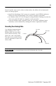

29
Publication 1763-IN001B-EN-P - September 2007
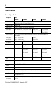
Working Voltage
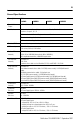
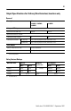
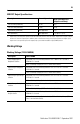
Turn-On Time (maximum) 0.1 ms 6 µs
Turn-Off Time (maximum) 1.0 ms 18 µs
Repeatability (maximum) Not Applicable 2 µs
Drift (maximum) Not Applicable 1 µs per 5 °C (9 °F)
(1)
Output 2 and 3 are designed to provide increased functionality over the other FET outputs. Output 2 and 3 may be used like
the other FET transistor outputs, but in addition, within a limited current range, they may be operated at a higher speed.
Output 2 and 3 also provide a pulse train output (PTO) or pulse width modulation output (PWM) function.
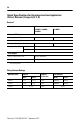
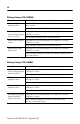
Working Voltage (1763-L16AWA)
Description 1763-L16AWA
Power Supply Input to
Backplane Isolation
Verified by one of the following dielectric tests: 1836V ac for 1 second or
2596V dc for 1 second
265V ac Working Voltage (IEC Class 2 reinforced insulation)
Input Group to Backplane
Isolation
Verified by one of the following dielectric tests:1517V ac for 1 second or
2145V dc for 1 second
132V ac Working Voltage (IEC Class 2 reinforced insulation)
Input Group to Input Group
Isolation
Verified by one of the following dielectric tests:1517V ac for 1 second or
2145V dc for 1 second
132V ac Working Voltage (basic insulation)
Output Group to Backplane
Isolation
Verified by one of the following dielectric tests: 1836V ac for 1 second or
2596V dc for 1 second
265V ac Working Voltage (IEC Class 2 reinforced insulation)
Output Group to Output
Group Isolation
Verified by one of the following dielectric tests: 1836V ac for 1 second or
2596V dc for 1second
265V ac Working Voltage (basic insulation), 150V ac Working Voltage (IEC
Class 2 reinforced insulation)
BBB FET Output Specifications
Description General Operationl
High Speed Operation
(1)
(Output 2 and 3 Only)