SLC 500 Fast Analog I/O Module Catalog Numbers 1746-FIO4I and 1746-FIO4V User Manual
Important User Information Solid state equipment has operational characteristics differing from those of electromechanical equipment. Safety Guidelines for the Application, Installation and Maintenance of Solid State Controls (publication SGI-1.1 available from your local Rockwell Automation sales office or online at http://literature.rockwellautomation.com) describes some important differences between solid state equipment and hard-wired electromechanical devices.
Table of Contents Preface About This Publication . . . . . Who Should Use This Manual Additional Resources. . . . . . . Conventions . . . . . . . . . . . . . . . . . . . . . . . . . . . . . . . . . . . . . . . . . . . . . . . . . . . . . . . . . . . . . . . . . . . . . . . . . . . . . . . . . . . . . . . . . . . . . . . . . . . . . . . . . . . . . 5 5 6 6 Chapter 1 Quick Start Required Tools and Equipment . . . . . . . . . . . . . . . . . . . . . . . 7 Procedures . . . . . . . . .
Table of Contents Chapter 6 Calibrate the Module Calibration Tradeoffs . . . . . . . . . . . . . . . . . . . . . . . . . . . . . . 61 Calibrate an Analog Input Channel . . . . . . . . . . . . . . . . . . . 62 Chapter 7 Test Module Operation Test the SLC 500 System . . . . . . . . . . . . . . . . . . . . . . . . . . . 67 Test the Module . . . . . . . . . . . . . . . . . . . . . . . . . . . . . . . . . 67 Chapter 8 Maintenance and Safety Preventive Maintenance. . . . . . . . . . . . . . . . . . . . .
Preface About This Publication Read this preface to familiarize yourself with the rest of the manual. This preface covers the following topics: • • • • • Who should use this manual The purpose of this manual Terms and abbreviations Conventions used in this manual Allen-Bradley support This manual is a reference guide for the 1746-NR4 RTD/Resistance Input Module. The manual: • gives you an overview of system operation.
Preface Additional Resources The following documents contain information that may be helpful to you as you use Allen-Bradley SLC products.
Chapter 1 Quick Start This chapter presents an overview of installation and start-up procedures to help you get the module working quickly. It refers to full procedures in corresponding chapters of this manual or in other SLC documentation that may be helpful if you are unfamiliar with programming techniques or system installation. We recommend that you use this chapter in either of two ways. • Use as a fast installation and start-up guide for the experienced users.
Quick Start Procedures Follow these steps to get your module running in your SLC system. 1. Plan the inclusion of analog I/O modules in your SLC system. If a new system, specify the type of processor, number of I/O racks, I/O modules, and power supply. If adding to an existing system: • assign modules to slot locations in the I/O rack. • verify that the power supply for the I/O rack can handle the increased load. See SLC 500 Systems Selection Guide, publication 1747-SG001, for more information. 2.
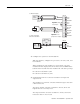
Quick Start 9 For Differential Inputs Module Analog + Sensor – Earth Ground Important: Jumper unused inputs. Load Earth Ground Important: Do not jumper unused outputs. For Single-ended Input with 3-wire Transmitter Transmitter Supply Signal GND 0 1 2 IN 0 + IN 0 – ANL COM 3 4 5 IN 1 + IN 1 – ANL COM 6 7 8 Not Used OUT 0 ANL COM 9 10 11 Not Used OUT 1 ANL COM Module Power + Supply – 3 4 5 IN + IN – ANL COM 4. Configure the system I/O and module ID.
Quick Start The lowest two bits have no effect on the output value. Refer to Processor and Module Considerations on page 29 for more information. SLC 500 Processor Data Files Input Image (2 words) Address Channel 0 Input Word I:1.0 Channel 1 Input Word I:1.1 Output Image (2 words) lsb msb (variable input data) 0 0 0 0 Bit 15 Bit 11 Bit 0 Address O:1.0 Channel 0 Output Word Channel 1 Output Word O:1.1 msb variable output data) lsb X X Bit 2 Bit 0 Bit 15 X = not used 6.
Chapter 2 Install and Wire the Modules This chapter describes procedures to install fast analog I/O modules in an SLC 500 system. The procedures include the following tasks.
Install and Wire the Modules Determine Compatibility with Other I/O Modules Use the I/O Compatibility chart when using the expansion rack of a fixed controller (1747-L20, 1747-L30, and 1747-L40). The chart determines compatibility of other I/O modules with fast analog modules. Compatibility is solely based on current drawn from the backplane. For more information, refer to the SLC 500 Fixed Hardware Style Installation and Operation Manual, publication 1747-6.21.
Install and Wire the Modules 13 I/O Compatibility 1746-FIO4I 1746-FIO4V 1746 Module • OW4 OW8, OW16 OX8 • BASIC BASn DCM HS • KE KEn Configure Input Channels (1) The • symbol indicates an allowable combination of 1746 I/O modules. (2) The ∇ symbol indicates an auxiliary 24V dc power supply may be needed. Your fast analog I/O modules have a two-switch assembly to configure the input channels for either current or voltage operation. The switches are on the module’s circuit board.
Install and Wire the Modules Select the I/O Rack Slot Two factors determine where you should locate the module in the I/O rack: ambient temperature and electrical noise. Consider the following conditions when selecting an I/O rack slot for the module. Position the module: • in a slot away from ac or high voltage dc modules. • away from the rack power supply if installed in a modular system. • in the I/O rack lowest in the enclosure for a cooler ambient.
Install and Wire the Modules 15 4. To remove the module, press the retaining clips at the top and bottom of the module and slide the module out. Installing the Module Card Guide Self-locking tabs secure the module in the I/O rack.
Install and Wire the Modules Considerations When Wiring This section provides guidelines on wiring the system, grounding the cables, determining cable length. ATTENTION Before wiring the module, disconnect SLC system power, I/O rack power, and module power. System Wiring Guidelines Use the following guidelines in planning the system wiring to the module. • Analog common terminals (ANL COM) are electrically interconnected inside the module, but not internally connected to earth.
Install and Wire the Modules 17 Ground the Cable Signal cable such as Belden cable #8761 (or equivalent) has two signal wires (black and clear), one drain wire, and a foil shield. The drain wire and foil shield must be grounded at only one end of the cable, not at both ends.
Install and Wire the Modules Minimize Electrical Noise Interference Because high-speed analog signals are particularly vulnerable to electrical noise, take precautions when routing your signal cables. To help reduce the effects of electrical noise on analog signals, we recommend that you do the following: • • • • • Install the SLC 500 system in a NEMA rated enclosure. Make sure that the SLC 500 system is properly grounded. Use Belden cable #8761 (or equivalent) for signal wiring.
Install and Wire the Modules 19 3. Apply shrink wrap where wires leave the casing with the hot-air blower. 4. Cut off the drain wire and foil shield at the other end of the cable. 5. Apply shrink wrap to the junction where wires leave the casing. 6. Trim the signal wires to 5 cm (2 in.) lengths. Strip about 4.76 mm (3/16 in.) of insulation away to expose the copper strands for your connections. 7. Decide where you will connect the cable to earth ground, and ground it. Refer to Ground the Cable on page 17.
Install and Wire the Modules IMPORTANT Single-ended inputs are less immune to noise than are differential inputs. Wiring Schematic for Single-ended Current-loop Analog Input Connections Important: The module does not provide loop power for analog inputs. Use a power supply that matches the transmitter specifications.
Install and Wire the Modules Label the Terminal Block 21 The terminal block has a write-on label. Use it to ensure that you install the correct terminal block on the corresponding module. Terminal Block Note: The black dot on the label indicates the position of terminal 0.
Install and Wire the Modules Publication 1746-UM009B-EN-P - September 2007
Chapter 3 Access Files to Configure I/O There are two ways to configure the SLC Chassis for a 1746-FIO4I/V module. You can either click and drag items from the list or you can use the Read IO Config method. Click and Drag Configuration Follow these steps to configure the SLC chassis by clicking and dragging modules. 1. Double-click the menu item to open the IO Configuration menu in RSLogix500 software. 2. Place the 1746-FIO4I/V module into the correct slot by clicking and dragging from the list.
Access Files to Configure I/O The I/O Configuration is now complete. Each slot shows the corresponding module that is located on the rack. In this example the 1746-FIO4V is in slot 1. Read IO Config Method Follow these steps to configure the SLC chassis by using the Read IO configuration method. 1. Double-click the menu item to open the IO Configuration menu in RSLogix500 software.
Access Files to Configure I/O 25 2. Place the 1746-FIO4I/V module into the correct slot by clicking Read IO Config. The following screen appears. 3. Select either the driver and processor node number or use the Who Active button to browse for the device. • If you selected the driver and node number, proceed to step 5. • If you clicked Who Active, the following screen appears.
Access Files to Configure I/O The Who Active screen lets you browse for the SLC device. 4. Locate the SLC Chassis under the appropriate driver and click OK. You are brought back to the Read IO Config screen. 5. Click Read IO Config and the rack is populated automatically.
Access Files to Configure I/O 27 The I/O Configuration is now complete. Each slot shows the corresponding module on the rack. In this example the 1746-FIO4V is in slot 1.
Access Files to Configure I/O Publication 1746-UM009B-EN-P - September 2007
Chapter 4 Processor and Module Considerations This chapter describes concepts that you need to understand to program the fast analog I/O module in an SLC 500 system. The following are processor considerations. • Update processor analog I/O data • Monitor analog I/O data • Address I/O image words The following are module considerations.
Processor and Module Considerations Processor Considerations Knowing how the processor works helps you program it more effectively. Processor Update of Analog I/O Data Analog input and output image words are updated by the processor once every processor scan when the processor scans data and program files in succession. Processor scan time depends largely on the size of your program files: the greater the number of programming instructions, the longer the time to scan the file.
Processor and Module Considerations 31 Address I/O Image Words Each module input channel is addressed as a single word in the processor’s input image table and each module output channel is addressed as a single word in the processor’s output image table. The module uses a total of two input words and two output words. Processor I/O Image Words Used by the Module Word Addresses in I/O Image File Bit 15 Output Image Analog Input Sensors Bit 15 Output Scan O:e.0 O:e.
Processor and Module Considerations Module Considerations The module’s I/O channel converters affect resolution of I/O data and bit usage in I/O image words. We show you how to compute I/O signal levels. Input filtering and input A/D conversion affect input response time. Data Resolution of the Module’s I/O Channel Converters The module’s I/O channel converters limit bit usage to less than a full 16-bit word when converting analog to digital input data and digital to analog output data.
Processor and Module Considerations 33 Convert Analog Input Data The module converts analog input signals to 12-bit binary values for storage in the input image table. The decimal range, number of significant bits, and converter resolution depend on the input range that you use for the channel. Input Range Decimal Range (input image table) Significant Bits 0…10V – 1LSB 0…4095 12 0…5V 0…2047 11 1…5V 409…2047 10 0…20 mA 0…2047 11 4…20 mA 409…2047 10 Nominal Resolution 2.4414 mV/LSB 9.
Processor and Module Considerations For example, if the input image table value is 409 from a 4…20 mA sensor. EXAMPLE Full Scale Input Sensor Signal = Full Scale Count x Input Image Value = 0.00977 x 409 = 4 mA Convert Analog Output Data The module converts 16-bit binary values from the output image table to 14-bit analog output signals and left-justifies the bit code in the channel word.
Processor and Module Considerations If the module’s output range is 4…20 mA and you want to set the output to 4 mA, compute the output image value as follows. EXAMPLE Output Image Value = 31,208 ~ 20 mA x 4 mA – 6242 The actual resolution for analog current outputs is 2.56348 µA/LSB, where the 14-bit decimal representation is left justified as follows.
Processor and Module Considerations Input Channel Filtering The module’s input filters are designed to attenuate less than 1% of the input signal in the 0…1000 Hz range. Percent of Signal Passed 100 99.9 99.8 Percent of Signal 99.7 99.6 99.5 99.4 99.3 99.2 99.1 99 0 100 300 500 1000 The –3dB point is approximately 7000 Hz. The input filter causes a signal delay of approximately 100 µs. The module’s A/D converter sees a 95% step change of an input signal in that time.
Processor and Module Considerations 37 Time Delay for A/D Conversion The A/D converter uses 7.5 µs for data conversion, 248.5 µs for data settling, and 256 µs for data transfer to the backplane. New data is available in 512 µs cycles. Response Time of A/D Converter Start Data conversion Data settling 7.5 µs 248.5 µs Data transfer to the backplane Data ready for processor read 256 µs 512 µs Worst case point for a change of input to occur. This results in a 1.
Processor and Module Considerations Input Response to Slot Disable The module continues to update its inputs for transfer to the processor, but the processor: • does not read inputs from the module in a disabled slot. • retains the last-state input image table values. • upon re-enabling the slot, reads current inputs in the subsequent scan. Output Response to Slot Disable While the module holds its outputs in their last state, the processor: • may update its output image table.
Chapter 5 Write Ladder Logic This chapter presents these programming examples. • • • • • • Retentive and non-retentive programming Detect an out-of-range input Scale analog inputs and detect an out-of-range condition Scale analog outputs Scale offsets when > 32,767 or < –32,768 Scale and range-check analog inputs and outputs • PID xontrol with analog I/O scaling IMPORTANT Retentive and Non-retentive Programming We present programming examples for instructional purposes only.
Write Ladder Logic We give you the following examples for programming a different response. • Retentive analog output • Non-retentive analog output • Clear the output for changing mode or cycling power Retentive Analog Output This example loads a program constant into an analog output channel. Consider a digital I/O module in slot 1, and an analog I/O module in slot 2.
Write Ladder Logic 41 Clear the Output for Changing Mode or Cycling Power This example clears analog output channel 0 during the initialization scan (first processor scan). The first pass bit, S2:1/15, in the Status File is used to initialize the analog output when you apply power in the RUN mode or upon setting the processor to the RUN or TEST mode. This bit goes ON automatically only for the first-pass scan.
Write Ladder Logic We present an alternative program for SLC 5/02 (and later) processors. It uses a single Limit Test instruction that checks low and high limits. Whenever the input value exceeds a limit, this program latches a bit that could trigger an alarm elsewhere in your ladder program. In this example, the input range is 0…10V dc (decimal range of 0…4095). If the input range were 4…20 mA, the low and high limits would be 2047 and 408, respectively.
Write Ladder Logic 43 We illustrate input and output scaling, the source and type of data to be scaled, and the type and destination of the scaled data.
Write Ladder Logic Scale an Analog Input and Detect an Out-of-range Condition The following example shows input range checking and scaling the analog input to engineering units for a 1746-FIO4V analog input module. We are making the following assumptions: • The 1746-FIO4V module is located in slot 3 of a modular system. • A pressure sensor with a 0…10V dc output is wired to input channel 1. • The sensor signal voltage is proportional to a range of 100…500 PSI.
Write Ladder Logic 45 Calculate the Linear Relationship Use the following equations to express the linear relationship between the input value and the resulting scaled value. Scaled value = (input value x slope) + offset Slope = (scaled max – scaled min) / (input max – input min) (500 – 100) / (4095 – 0) = 400/4095 = 0.0977 Offset = scaled min – (input min x slope) (100 – (0 x [400/4095]) = 100 Scaled value = (input value x [0.
Write Ladder Logic Standard Math Example Rung 2:0 Check for below range Rung 2:1 Check for above range LES LESS THAN Source A Source B MUL MULTIPLY Source A Source Dest Multiply by the scaled range Clear fault bit from overflow DDV DOUBLE DIVIDE Source A Dest Divide result by input range Rung 2:3 I:3.1 1750 GRT GREATER THAN Source A I:3.
Write Ladder Logic Scale an Analog Output 47 This example shows the scaling of analog output values to engineering units for monitoring or controlling purposes. We are making these assumptions. • The FIO4I module is located in slot 2 of an SLC 500 system. • An actuator of a flow control valve is wired to output channel 0. • The actuator accepts a 4…20 mA signal for a 0…100% of valve opening. • The actuator can not receive a signal out of the 4…20 mA range.
Write Ladder Logic Ladder Logic The out-of-range limits are predetermined because any value less than 0% is 6242 and any value greater than 100% is 31,208. The ladder logic checks for out-of-range limits to verify that not less than 4 mA and not more than 20 mA is delivered to the analog output channel. The following ladder logic uses standard math. It unlatches the mathematical overflow bit S2:5/0 before the end of the scan to prevent a processor fault.
Write Ladder Logic Scale Offsets When >32,767 or <32,768 49 Some applications may produce an offset greater than 32,767 or less than –32,768, the largest value that can be stored in a 16-bit integer or processed by an SLC processor. If so, you may reduce the magnitude of the offset by shifting the linear relationship along the input value axis. When you compute linear relationships, you will see how the offset is reduced in this manner. The following example applies to a 0.5…9.
Write Ladder Logic 2. Then we shift the linear relationship along the input value axis. 9.5 V = 3890 (scaled max) Scaled Value 0.5 V = 205 (scaled min) 90% (input min) 100% (input max) Input Value 3. Now we compute the offset for the shifted linear relationship. Offset = scaled min – (input min x slope) = 205 – [0 x (368.5)] = 205 The offset is 205, well below 32,767. The slope remains 3685/10 (> 3.2767), so you cannot use the SCL instruction for scaling.
Write Ladder Logic 51 Ladder Logic The following ladder logic uses standard math. It unlatches the mathematical overflow bit S2:5/0 before the end of the scan to prevent a processor fault. The module is located in slot 2, and the output device is wired to channel 0.
Write Ladder Logic Range-check an Analog Input and Scale It for an Output This example checks the range of an analog input and scales it for use as an output. An 1746-FIO4V module is placed in slot 1 of an SLC 500 system. A 4…20 mA signal representing 0…200 PSI from a pressure sensor is delivered to input channel 0. The input value is checked to ensure it remains within range. If the ladder logic detects an out-of-range condition, it sets a flag bit.
Write Ladder Logic 53 Ladder Logic We present two examples. The first runs on any SLC 500 processor. The second uses the scaling instruction available on SLC 5/02 (and later) processors. In the first example, the analog input value is checked against the minimum and maximum input limits. B3:0/0 is the in-range flag bit. If the input is out of range, the in-range flag bit is reset and the output is set to its minimum or maximum limit.
Write Ladder Logic Example Program for Any SLC Processor Rung 2:0 Set in-range bit B3/0 (L) Rung 2:1 Check for below range LES LESS THAN Source A Source B MOV MOVE I:1.0 409 Rung 2:2 Check for above range GRT GREATER THAN Source A Source B Source Dest B3/0 (U) MOV MOVE I:1.
Write Ladder Logic Rate Rate Rate Rate Rate = = = = = 55 slope x 10,000 (scale range / input range) x 10,000 3276 / 1638 x 10,000 2 x 10,000 20,000 If the slope was greater than 3.2767, you could not use the SCL instruction because the rate would exceed 32,767, a value too large to handle.
Write Ladder Logic PID Control with Analog I/O Scaling With the combination of PID and SCL (scale) instructions or PID and standard math instructions, you can write and display ladder logic in engineering units such as PSI or °C. Follow these steps to display ladder logic in engineering units. 1. Scale the analog input PV by calculating the slope (or rate) of the analog input range. For example, an input range such as 1…5V dc has a corresponding scaled range of 409…2047.
Write Ladder Logic 57 3. Enter PID parameters in engineering units into the PID instruction. For example, if the 4…20 mA analog input range represents 0…300 PSI, enter 0 as the minimum (Smin) and 300 as the maximum (Smax). You can also enter setpoints and deadband in engineering units. The data monitor screen for PID displays its parameters in the same engineering units. Ladder Logic We present two examples of PID control logic with analog I/O scaling for use on an SLC 5/02 (or later) processor.
Write Ladder Logic Example Program for SLC 5/02 (or later) Processors (scaled voltage input and output) IIM IMMEDIATE INPUT w MASK Slot I:1.0 Mask FFFF Length 1 Rung 2:0 MUL MULTIPLY Source A Source B Dest Rung 2:1 Rung 2:2 PID PID Control Block Process Variable Control Variable Control Block Length Rung 2:3 SCL SCALE Source Rate (/10000) Offset Dest Rung 2:4 Rung 2:5 Publication 1746-UM009B-EN-P - September 2007 I:1.0 4 N7:0 0 N10:0 N7:0 N10:29 23 N10:29 0 19999 0 O:1.
Write Ladder Logic 59 Example Program for SLC 5/02 (or later) Processors (scaled current input and output) Rung 2:0 IIM IMMEDIATE INPUT w MASK I:1.0 Slot Mask FFFF Length 1 Rung 2:1 Scale the analog input with math instructions. Multiply by scaled range MUL MULTIPLY Source A Source B Dest S2:5 (U) 0 Clear overflow fault bit Divide by input range Add offset I:1.
Write Ladder Logic Brake Monitor Example Program for SLC 5/02 (or later) Processors Rung 2:2 The next 2 rungs ensure that the analog input value to be scaled remains within the limits of 409 and 2047. This prevents out-of-range conversion errors in the SCL and PID instructions. The latch bits can be used elsewhere in the program to identify the particular out-of-range error which occurred.
Chapter 6 Calibrate the Module This chapter helps you calibrate the module’s analog input channels to increase the expected accuracy from ± 21 LSB of error to ± 6 LSB. The combination of calibration program and procedure is designed to reduce offset and gain errors by: • scaling the values read during calibration. • applying them during runtime. We provide example computations and ladder logic for your reference.
Calibrate the Module Calibrate an Analog Input Channel We provide an example calibration program and a calibration procedure to show you how to calibrate an analog input channel. This example assumes an analog output of 4…20 mA from a transducer. The corresponding decimal code that the module would write into the processor’s input image table would be 409 at 4 mA and 2047 at 20 mA if the overall error of an input channel were zero. However, the overall error of ± 0.
Calibrate the Module 63 These addresses are used in the example program. (Each channel requires its own program and separate addresses.) Example Program Addresses Bit or Value Address Cal_Lo I:1.0/0 and N10:0/0 (You set these bits in step 3.) Cal_Hi I:1.0/1 and N10:0/1 (You set these bits in step 4.) Calibrate I:1.0/2 and N10:0/2 (You set these bits in step 5.) Convert Enable N10:10/4 (Runtime enable) Analog_In I:2.
Calibrate the Module Rung 2:0 Cal_Lo I:1.0 ] [ 0 N10:0 [OSR] 0 MOV MOVE Source Dest Rung 2:1 Cal_Hi I:1.0 ] [ 1 N10:0 [OSR] 1 MOV MOVE Source Dest Rung 2:2 Calibrate I:1.
Calibrate the Module 65 MUL MULTIPLY Source A Source B Dest Lo_Value 400 Slope_x10K 9897 N10:5 32767 DDV DOUBLE DIVIDE Source Dest 10000 N10:6 396 SUB SUBTRACT Source A Source B Dest Scale_Lo 409 N10:6 396 Offset 13 S:5 (U) Rung 2:4 Convert Enable During Runtime 0 MUL N10:10 ] [ 4 MULTIPLY Source A Source B Dest Analog_In 1000 Slope_x10K 9897 N10:8 32767 S:5 (U) 0 DDV DOUBLE DIVIDE Source Dest 10000 N10:12 990 ADD ADD Source A Source B Dest N10:12 990 Offset 13 Analog_Scl 1003 Rung 2
Calibrate the Module Calibration Procedure Recalibrate every six months, or as necessary. 1. Let the module warm up under power for at least 20 minutes at ambient operating temperature. 2. Determine the scaled high and low values you wish to use in your application. In this example, scaled high is 2047 (20 mA) and scaled low is 409 (4 mA). 3. Capture the Lo calibration value. a. Place the input sensor (or input source) at the low (4 mA) position. b. Set the Cal Lo bit (I:1.0/0) and OSR bit (N10:0/0).
Chapter 7 Test Module Operation This chapter helps you test the operation of the module’s I/O channels. Test the SLC 500 System Testing the SLC 500 system is beyond the scope of this manual. We mention it here only because you should test and debug at the system level before testing and debugging the module in the system.
Test Module Operation Inspect Module Switches and Wiring Inspect the module as follows before installing it. 1. Set the input configuration switches 1 and 2 correctly. 2. Check that wiring connections are OK and no wires are missing or broken. 3. Tighten terminal connections to secure the wires. ATTENTION Care should be taken to avoid connecting a voltage source to a channel configured for a current input. Improper module operation or damage to the module can occur. 4.
Test Module Operation 69 Leave the module connected to the output device to serve as the output load where possible, but inhibit its affect on controlling the process. Substitute a passive load for the active device as an alternative. ATTENTION Process operation during system checkout can be hazardous to personnel. During checkout procedures, disconnect, inhibit, or substitute a passive load for all devices which, when energized, might cause the process to operate.
Test Module Operation Test Analog Inputs Before testing the module’s input channels, the SLC 500 system must be installed and tested according to the SLC 500 Modular Hardware Style User Manual, publication 1747-UM011. The processor must be connected to a programming device, properly configured, and must have no rungs in its ladder program. The module’s LED indicator must also be illuminated.
Test Module Operation 71 3. With the programming device on-line, select the processor’s Test- Continuous scan mode. This provides a safer testing mode because outputs are not energized. 4. Display the data in File 2 (Input Image table). 5. Select the Data Monitor mode of your programming device when viewing I/O point I:1.0. 6. Change the radix of the display to decimal. 7. If the sensor is connected, set it to its lower limit.
Test Module Operation Test Analog Outputs Before testing the module’s output channels, the SLC 500 system must be installed and tested according to the SLC 500 Modular Hardware Style User Manual, publication 1747-UM011. The processor must be connected to a programming device, properly configured, and must have no rungs in its ladder program. The module’s LED indicator must also be illuminated.
Test Module Operation 73 5. Download the test rung to the processor and select RUN mode. 6. Display the data in address N7:0. 7. Enter the lower limit in N7:0. For example, if the lower limit is 1 volt, enter 3277 into N7:0. 8. Check that the output device is connected to the output channel and that the device assumes its lower limit condition. If the output device is disconnected, read the replacement meter. Do not overlook module and meter errors. 9. Enter the upper limit in N7:0.
Test Module Operation Publication 1746-UM009B-EN-P - September 2007
Chapter 8 Maintenance and Safety This chapter provides preventive maintenance information and safety considerations when troubleshooting your SLC 500 system. Preventive Maintenance The printed circuit boards of the analog modules must be protected from dirt, oil, moisture, and other airborne contaminants. To protect these boards, the SLC 500 system must be installed in an enclosure suitable for the environment.
Maintenance and Safety Safety Considerations When Troubleshooting Safety considerations are an important element of proper troubleshooting procedures. Actively thinking about the safety of yourself and others, as well as the condition of your equipment, is of primary importance. Refer to the Installation and Operation Manual for Fixed Hardware Style Programmable Controllers, publication 1747-6.
Appendix A Module Specifications General Description The 1746-FIO4I and 1746-FIO4V fast analog I/O modules provide two input and two output channels. Input channels are the same for both types of modules: you select either current or voltage operation for each channel. The 1746-FIO4I module contains two current-output channels, while the 1746-FIO4V module contains two voltage-output channels.
Module Specifications Electrical Specifications - 1746-FIO4I, 1746-FIO4V Attribute Value Noise Immunity NEMA standard ICS 2-230 Temperature, Operating 0… 60 °C (32…140 °F) Temperature, Storage –40…85 °C (–40…185 °F) Relative Humidity 5 … 95% (noncondensing) General Input Specifications - 1746-FIO4I, 1746-FIO4V Attribute Value Converter Resolution 12 bits Converter Type Successive approximation Track and Hold Time to Acquire the Analog Signal Before Conversion 1.
Module Specifications 79 Voltage Input Specifications - 1746-FIO4I, 1746-FIO4V Attribute Value Overall Accuracy at 25 °C (77 °F) ±0.440% of full scale Overall Accuracy at 60 °C (140 °F) ±0.750% of full scale Overall Accuracy Drift ±88 ppm/°C (max) Gain Error at 25 °C (77 °F) ±0.323% of full scale Gain Error at 0…60 °C (32…140 °F) ±0.
Module Specifications Current Output Specifications for 1746-FIO4I Publication 1746-UM009B-EN-P - September 2007 Attribute Value Converter Resolution 14 bit Location of LSB in I/O Image Word 0000 0000 0000 01XX Non-linearity 0.05% of full scale (max) Conversion Method R–2R ladder Step Response 2.
Module Specifications 81 Voltage Output Specifications for 1746-FIO4V Attribute Value Converter Resolution 14 bit Location of LSB in I/O Image Word 0000 0000 0000 01XX Non-linearity 0.05% of full scale Conversion Method R–2R ladder Step Response (to 95%) 2.5 ms (normal) Load Range 1 k…∞Ω Load Current 10 mA (max) Load Reactance 1 µF (max) Voltage Output Coding (–10…10V dc – 1 LSB) –32,768 … +32,764 Output Range –10 … 10V – 1 LSB (normal) Resolution 1.
Module Specifications Publication 1746-UM009B-EN-P - September 2007
Appendix B 2’s-complement Binary Numbers Use 2’s-complement Binary Numbers The SLC 500 processor stores data as 16-bit binary numbers. The processor uses 2’s-complement binary format when making mathematical computations and when storing analog values in the I/O image table. As indicated in the figure on next page, the equivalent decimal value of the 2’s-complement binary number is the sum of corresponding position values.
2’s-complement Binary Numbers Positive Decimal Values The far left position is always 0 for positive values. Binary notation and 2’s-complement binary notation are identical for positive values. This format limits the maximum positive value to 32767 when all positions are 1 except for the far left position (see figure below). Study these examples.
2’s-complement Binary Numbers 85 Negative Decimal Values The far left position is always 1 for negative values. The equivalent decimal value of a negative 2’s-complement binary number is obtained by subtracting 32768 from the sum of the other position values. In the figure below, all positions are 1 and the value is 32767 – 32768 = –1.
2’s-complement Binary Numbers Publication 1746-UM009B-EN-P - September 2007
Appendix C Module Input and Output Circuits These wiring diagrams show the input circuit, voltage output, and current output for the fast analog modules. Input Circuit for 1746-FIO4V and 1746-FIO4I Modules 500K 33pF IN – > IN + > ANL COM > 500K S1, S2 – Filter 500K 250 Ω > A to D + 33pF 500K Switches S1 and S2 control whether the input circuit is for current (closed) or voltage (open). Voltage Output Circuit for 1746-FIO4V Modules Positive Voltage Supply 0.022 µF R1 from > DAC – R2 30K 0.
Module Input and Output Circuits Current Output Circuit for 1746-FIO4I Modules Positive Voltage Supply Ref ANL > COM R2 0.1 µF R1 – from > DAC Publication 1746-UM009B-EN-P - September 2007 Amp + 4.
Index Numerics 2’s complement binary numbers 83 negative decimal values 85 positive decimal values 84 A address I/O image words 31 analog output scale 47 C calculate linear relationship 45, 47 calculate out of range limits 45 calibrate analog input channel 62 calibration procedure 66 example program 62 calibrate the module 61 calibration tradeoffs 61 clear output 41 compatibility with other I/O modules 12 compute analog input signal level 33 compute analog output 34 configure I/O access 23 configure input
Index N non-retentive analog output 40 non-retentive programming 39 P PID control with analog I/O scaling 56 ladder logic 57 power requirements determine 11 power up the I/O rack 69 preventive maintenance 75 processor considerations 29 address I/O image words 31 monitor analog I/O data 30 update of analog I/O data 30 processor update of analog I/O data 30 S safe state for outputs 38 safety considerations when troubleshooting 76 scale analog input 44 calculate linear relationship 47 ladder logic 48 sc
How Are We Doing? Your comments on our technical publications will help us serve you better in the future. Thank you for taking the time to provide us feedback. You can complete this form and mail (or fax) it back to us or email us at RADocumentComments@ra.rockwell.com Pub. Title/Type SLC 500 Fast Analog I/O Module Cat. No. 1746-FIO4I and 1746-FIO4V Pub. No. 1746-UM009B-EN-P Pub. Date September 2007 Part No. XXXXXX-XX Please complete the sections below.
PLEASE FASTEN HERE (DO NOT STAPLE) PLEASE FOLD HERE NO POSTAGE NECESSARY IF MAILED IN THE UNITED STATES BUSINESS REPLY MAIL FIRST-CLASS MAIL PERMIT NO.
Rockwell Automation Support Rockwell Automation provides technical information on the Web to assist you in using its products. At http://support.rockwellautomation.com, you can find technical manuals, a knowledge base of FAQs, technical and application notes, sample code and links to software service packs, and a MySupport feature that you can customize to make the best use of these tools.