
Instruction Sheet User guide

B–7Smart Communication Card Data Tables
Publication
1403-5.1
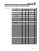
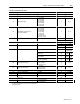
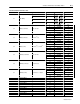
RangeWord No.Master Module RangeParameter NameParameter No.
28
10
±
0
to
21
4.14 3–Phase Average Voltage (L–L) 0 to 9999x10
21
volts 29 0 to 9999
30
10
±
0
to
21
4.15 Positive Sequence Voltage 0 to 9999x10
21
volts 31 0 to 9999
32
10
±
0
to
21
4.16 Negative Sequence Voltage 0 to 9999x10
21
volts 33 0 to 9999
34
10
±
0
to
21
4.17 Percent Voltage Unbalance 0.0 to 100.0 35 0 to 9999
36
10
±
0
to
21
4.18 L1–N Voltage 0 to 9999x10
21
volts 37 0 to 9999
38
10
±
0
to
21
4.19 L2–N Voltage 0 to 9999x10
21
volts 39 0 to 9999
40
10
±
0
to
21
4.20 L3–N Voltage 0 to 9999x10
21
volts 41 0 to 9999
42
10
±
0
to
21
4.21 3–Phase Average Voltage (L–N) 0 to 9999x10
21
volts 43 0 to 9999
44
10
±
0
to
21
422
Average Frequency
20 0 to 132 0
45 0 to 9999
4.22 Average Frequency 20.0 to 132.0
46
10
±
0
to
21
4.23 Last Cycle Frequency 20.0 to 132.0 47 0 to 9999
48
10
±
0
to
21
4.24 Phase Rotation
0 = No Rotation
1 = ABC
2 = ACB
49 0 to 2
Reserved Word 50
Reserved Word 51
Reserved Word 52
4.25 Data Format
0 = Integer/Exponent
1 = Floating Point
53 0 to 1
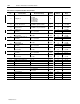
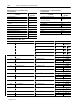
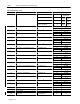
Table B.8 Real Time Power Data – Read
Parameter No. Parameter Name Master Module Range Word No. Range
5.1 Time Stamp Year 1
0–99
16 Bit Integer
Month, Date 2
1–12
8 Bit
1–31
8 Bit
Hour, Minute 3
0–23
8 Bit
0–59
8 Bit
Seconds, Hundredths 4
0–59
8 Bit
0–99
8 Bit
5.2 L1 Real Power 0 to 9999x10
21
W 5 0 to 9999
6
10
±
0
to
21
5.3 L2 Real Power 0 to 9999x10
21
W 7 0 to 9999
8
10
±
0
to
21
5.4 L3 Real Power 0 to 9999x10
21
W 9 0 to 9999
10
10
±
0
to
21
5.5 Total Real Power 0 to 9999x10
21
W 11 0 to 9999
12
10
±
0
to
21
5.6 L1 Reactive Power 0 to 9999x10
21
VAR 13 0 to 9999
14
10
±
0
to
21