
Instruction Manual

Firmware Block Diagrams A–5
Publication 1397-5.0 — June, 2001
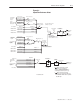
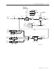
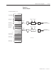
Figure A.5
Outer Control Loop
OCL Ref
Source
(P. 301)
*REGISTER
OCL Reference TP
(P. 020)
OCL Ramp
Output
(P. 019)
NOTES:
1>The –_oct_
–
enable signal must be
ON in order for the Outer Control
Loop to execute. When _ocl_ enable
is OFF, the S–curve Lead/Lag and PI
blocks are held in reset causing the
initial value (INITV) to be copied to
each block’s output.
2> The OCL reference ramp block
can be bypassed by setting OCL
RAMP TIME to 0.0.
*Indicates default selection
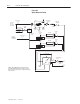
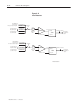
From
I/O Exp
Inputs Block
Diagram
–
+
MUL
OCL Reference
(P. 299)
ANLG IN 4
RATIO
OCL Enable TP
(P. 016)
*BYPASS
1> –OCL_enable
(to above)
FREQUENCY IN
ANLG IN 3
ADAPTOR 1–6
From SCANport
SCURVE
JERK
ACCDEC
RST\
OCL Ref
Rounding
(P. 300)
OCL Trim
Range
(P. 302)
OCL
Output
(P. 018)
INTV
–OCL–enable
(from below)
2> Ramp Time
(P. 298)
OCL Pos
Limit
(P. 296)
OCL Kp
(P. 294)
OCL
Lead
Freq
(P. 295)
OCL
Neg
Limit
(P. 297)
LOWLD
RST\
–OCL–
enable
(from below)
GAIN
INTV
KP HI
OCL
Lead/Lag
Type
(P. 293)
LEAD/LAG
LAG/LEAD
OCL
Lead/Lag
Ratio
(P. 292)
–OCL–
enable
(from below)
OCL
Lead/Lag
Freq
(P. 293)
INTV
L/L
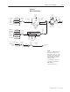
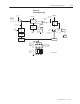
From
I/O Exp
Inputs Block
Diagram
(CML FEEDBACK)
8 sample average
ANLG IN 3
ANLG IN 4
CML FEEDBACK
FREQUENCY IN
From SCANport
OCL Fdbk
Source
(P. 290)
WLO
OCL Feedback
(P. 017)
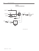
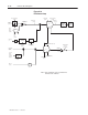
Outer Control Loop enable logic
OCL ENABLE LOGIC
REGISTER
OCL Enable
(CTB 64)
ADAPTOR 1–6
REGISTER
TERMBLK
OCL Enable TP
(P. 016)
Drive
Status
(P. 191)
OFF
Running
Not Running
RST\
0
To
A.6
OCL Fdbk Reg
(P. 304)