
Operating instructions


Page 2 RF Technology R350/R500
CONTENTS CONTENTS
Contents
1 Operating Instructions 4
1.1 Front Panel Controls and Indicators 4
1.1.1 Mon. Volume 4
1.1.2 Mon. Sq. 4
1.1.3 N. SQ 5
1.1.4 C. SQ 5
1.1.5 Line 5
1.1.6 PWR LED 5
1.1.7 SQ LED 5
1.1.8 Alarm LED 6
2 Receiver Internal Jumper Options 6
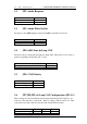
2.1 JP1: 240Hz Notch Filter 6
2.2 JP2: Audio Response 7
2.3 JP3: Audio Filter In/Out 7
2.4 JP4: 600Ω Line dc Loop COS 7
2.5 JP6: COS Polarity 7
2.6 JP7/8/9: dc Loop COS Configuration 7
2.7 JP7, JP8, JP9: Direct Output COS 8
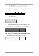
2.8 JP11 EPROM Type 8
2.9 JP13: Squelch Defeat (pcb 30/9132/0002 or later) 9
2.10 JP19: LED Alarm output (pcb 30/9132/0002 or later) 9
3 Receiver I/O Connections 10
3.1 25 Pin Connector 10
4 Channel and Tone Frequency Programming 11
5 Circuit Description 11
5.1 RF Section 11
5.2 IF Section 11
5.3 VCO Section 12
5.4 PLL Section 12
5.5 Audio Signal Processing 13
5.6 Noise Filter, Amplifier and Detector 13
5.7 Subtone Filter and CTCSS 13
5.8 External Squelch 14
5.9 Microprocessor Controller 14
5.10 Carrier Operated Switch 14
5.11 Voltage Regulator 15
6 Alignment Procedure 15
6.1 Standard Input Signal 15
6.2 RF Alignment 16
6.3 IF Alignment 17
6.4 Line Level Adjustment 17
6.5 Reference Oscillator Calibration 17