
User's Manual


Eclipse2 Technical Manual, 3-Aug-12 Page 13 of 17
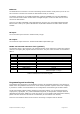
Channel 0: monitor speaker volume control
C
h
an
nel 1: 600 ohm audio Line input gain control
Channel 2: exciter reverse power of the power amplifier
Channel 3: AUX audio input bias setting
Channel 4: AUX audio output bias setting
Channel 5: receiver IF amplifier gain control (not used in release1 RX module)
Channel 6: exciter RF output power control
Channel 7: exciter VCO bias setting
Channel 8: receiver VCO bias setting
The op-amplifiers (U4, U28) are used for converting DAC output to proper voltage which is required
by the system hardware.
The Interface board accepts both TTL PTT input and E/M signaling, the TTL PTT is buffered by Q4
and Q5, E/M signal is isolated by Opto-coupler U3 to system I/O level. The output of the RISC I/O
logic is buffered by U1,Q1-Q3 for interfacing the external logic. The solid-state relay Opto-coupler
is used to isolate the system I/O from E/M signal.
A dual retriggerable monostable multivibrator (U5) in the circuit is functioned as a IRQ generator, it
senses the changes of the Input logic and sends a narrow pulse to the RISC processor for trigging
the processing IRQ.
U31 is a USB to RS232 bridge which transfers the USB data between the front panel connector and
the system serial bus. U9 is an transceiver which converts RS232 +/-15 logic from the rear panel
to serial bus level. U30 is a bus switch to select one of above passing through to the RSIC
processor.
Header (H4) is used only for emergency system booting purpose, do not assert jumper into this
header.
Clock generator
the 12.8MHz TCXO (X1) output is buffered (by U26) and divided by 4 (U29) to provides PLL
refe
rence frequency for exciter and receiver. The frequency doubler double 12.8MHz frequency to
25.6MHz to provide system clock for digital IF receiver.
Voltage regulators
There are nine voltage sources generated by the voltage regulator
VTX
– +12.5V DC for TX module
VRX – +12.0V DC for RX module
D3V3 – +3.3V DC for Processor (Master) board and 3V TTL logic
A3V – +3.15V DC for analog 3V rail
+12V – +12.0VDC for analog circuits
+5V – +5V DC for TCXO and 5V TTL logic
+1V8 – +1.8V DC for Flash core supply on the Processor (Master) board
-20V – -20.0V DC for TX and RX VCO bias setting
-12V – -12.0VDC for analog circuits
The input power supply voltage is 13.8VDC, LDO (U19, U22) provides 12.5V (Imax = 1.5A) and
12V DC (Imax = 800mA) for TX and RX module. Switch mode DC-DC converter (U20) generates
digital 3.3V DC rail (Imax=2A) for the Processor board and Interface board, then regulated to
3.15V analog DC rail by LDO (U21) for 3V analog circuits in the transceiver.
The DC-DC converter (U23) provides –20V negative supply voltage for VCO bias amplifier (U4).
Voltage regulator (U24) generates –12V DC supply analog circuits of the interface board.
RF modules