
Users Manual
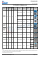
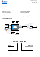


Table Of Contents
- TI CC264X BLE Module List
- 1 Device Overview
- Table of Contents
- Table of Figures
- Table of Tables
- 2 Module Configuration and Functions
- 3 Specifications
- 4 Application, Implementation, and Layout
- 5 Revision History
- 6 Contact Us

RF-BM-2642B1
www.szrfstar.com V1.0 - Jan., 2020
Shenzhen RF-star Technology Co., Ltd. Page 5 of 20
Table of Contents
TI CC264X BLE Module List .......................................................................................................................................... 2
1 Device Overview ............................................................................................................................................................. 3
1.1 Description............................................................................................................................................................ 3
1.2 Key Features ....................................................................................................................................................... 3
1.3 Applications .......................................................................................................................................................... 4
1.4 Functional Block Diagram .............................................................................................................................. 4
1.5 Part Number Conventions .............................................................................................................................. 4
Table of Contents ................................................................................................................................................................ 5
Table of Figures ................................................................................................................................................................... 6
Table of Tables ..................................................................................................................................................................... 6
2 Module Configuration and Functions ...................................................................................................................... 7
2.1 Module Parameters ........................................................................................................................................... 7
2.2 Module Pin Diagram ......................................................................................................................................... 8
2.3 Pin Functions ....................................................................................................................................................... 8
3 Specifications ................................................................................................................................................................. 10
3.1 Recommended Operating Conditions ..................................................................................................... 10
3.2 Handling Ratings .............................................................................................................................................. 10
3.3 Power Consumption ....................................................................................................................................... 10
3.3.1 Power Mode .......................................................................................................................................... 10
3.3.2 Radio Mode ........................................................................................................................................... 12
4 Application, Implementation, and Layout............................................................................................................. 13
4.1 Module Photos .................................................................................................................................................. 13
4.2 Recommended PCB Footprint .................................................................................................................... 13
4.3 Schematic Diagram ......................................................................................................................................... 14
4.4 Basic Operation of Hardware Design ...................................................................................................... 14
4.5 Trouble Shooting .............................................................................................................................................. 16
4.5.1 Unsatisfactory Transmission Distance ........................................................................................ 16
4.5.2 Vulnerable Module .............................................................................................................................. 16
4.5.3 High Bit Error Rate ............................................................................................................................. 16
4.6 Electrostatics Discharge Warnings ........................................................................................................... 16