


Resonant LLC Converter: Operation and Design
8
Application Note AN 2012-09
V1.0 September 2012
3 Design Steps
This section is to explain the impact of design parameters on voltage regulation and efficiency performance,
and facilitate the design and selection of such parameters. Our ultimate design objective it to achieve the
best performance while reaching the gain requirement for all line and load conditions. And for safe operation,
we must determine the minimum switching frequency the controller shall limit in order to maintain the
operation in the inductive region.
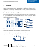
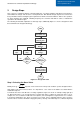
The following are detailed explanation of all design steps; additionally Figure 3.1 shows a design flow chart
that summarizes the design methodology.
Figure 3.1 Design flow chart
Step 1: Selecting the Qmax Value
Quality factor
ac
rr
R
CL
Q
depends on the load current. Heavy load conditions operate at high Q values,
while lighter loads have lower Q values. It is important to set a value for the Qmax associated with the
maximum load point.
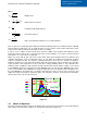
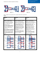
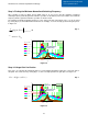
To illustrate the effect of the Q value on voltage regulation, Figure 3.2 shows an example voltage gain plot
for different Q values. Let’s assume that the resonant tank gain is required to range from 0.8 to 1.2 for
example, we can see that the low Q value curve (Q=0.3) can reach higher boost gain, but it is less sensitive
to frequency modulation in the “above resonance fs>fr” region, hence, switching frequency has to increase
much in order to reach the minimum voltage gain (K=0.8), causing extra switching losses, while the higher Q
START
Step 1:
Select Qmax value
Step 2:
Select m value
Step 3:
Find Fx
min
Step 4:
Find K
max
Is K
max
=
required gain?
Yes
Is K
max
<
required
gain?
Decrease m
value
Increase m
value
Yes
No
No
END
Step 5:
Solve for resonant
components values