


Resonant LLC Converter: Operation and Design
7
Application Note AN 2012-09
V1.0 September 2012
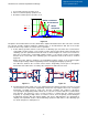
Figure
2
.
7
Figure
2
.
8
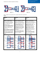
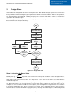
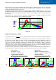
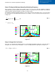
Table 1 explains the converter modes of operation and shows key waveforms
Table 1
At Resonant frequency
operation
fs=fr.
Above resonant frequency
operation
fs>fr.
Below resonant frequency
operation
fs<fr
Each half of the switching cycle
contains a complete power
delivery operation (described
above), where the resonant half
cycle is completed during the
switching half cycle.
By end of the switching half cycle,
the resonant inductor current I
Lr
reaches the magnetizing current
I
Lm
, and the rectifier current
reaches zero.
The resonant tank has unity gain
and best optimized operation and
efficiency, therefore, transformer
turns ratio is designed such that
the converter operates at this
point at nominal input and output
voltages.
Each half of the switching cycle
contains a partial power delivery
operation (described above),
similar to the resonant frequency
operation, but it differs in that the
resonant half cycle is not
completed and interrupted by the
start of the other half of the
switching cycle, hence primary
side MOSFETs have increased
turn off losses and secondary
rectifier diodes have hard
commutation.
The converter operates in this
mode at higher input voltage,
where a step down gain or buck
operation is required.
Each half of the switching cycle
contains a power delivery
operation (described above), at
the time when resonant half cycle
is completed and resonant
inductor current I
Lr
reaches the
magnetizing current, the
freewheeling operation (as
described above) starts and
carries on to the end of the
switching half cycle, hence
primary side have increased
conduction losses due to the
circulating energy.
The converter operates in this
mode at lower input voltage,
where a step up gain or boost
operation is required.
Cr Lr
Lm
Np
S1
S2
S3
S4
Ns
+
Vo
-
D1
D2
D3
D4
Cr Lr
Lm
Np
S1
S2
S3
S4
Ns
+
Vo
-
D1
D2
D3
D4
S
1
,S
4
S
2
,S
3
V
ds_S2,S3
Ts=1/fs
Ts/2
Vin
I
Lr
I
Lm
I
D1,D4
I
D2,D3
t
V
ds_S2,S3
Ts=1/fs
Ts/2
Vin
t
I
Lm
I
Lr
S
1
,S
4
S
2
,S
3
I
D1,D4
I
D2,D3
V
ds_S2,S3
Ts=1/fs
Ts/2
Vin
Tr/2
t
I
Lm
I
Lr
S
1
,S
4
S
2
,S
3
I
D1,D4
I
D2,D3