


Resonant LLC Converter: Operation and Design
5
Application Note AN 2012-09
V1.0 September 2012
Where,
ac
rr
R
CL
Q
Quality factor
o
S
P
ac
R
N
N
R
2
2
2
8
Reflected load resistance
r
s
x
f
f
F
Normalized switching frequency
rr
r
CL
f
2
1
Resonant frequency
r
mr
L
LL
m
Ratio of total primary inductance to resonant inductance
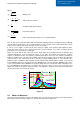
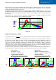
One can plot the resonant tank gain K with the normalized switching frequency for different values of Quality
factor Q and any single value of m, as shown in Figure 2.3. The selection of the m value will be discussed in
a later section of this document, but m=6 was used as an example.
It can be seen in Figure 2.3 that low Q curves belong to lighter load operation while higher Q curves
represent heavier loads. It’s also seen that all Q curves (load conditions) cross at the resonant frequency
point (at Fx=1 or fs=fr) and have a unity gain.
Figure 2.3 shows that all gain curves has peaks which define the boundary between the inductive and
capacitive impedances of the resonant tank, hence we can define the inductive and capacitive operation
regions as shaded in the plot, the objective of defining both regions is because it is desired to maintain an
inductive operation across the entire input voltage and load current ranges, and never fall into the capacitive
region operation. Such requirement is due to that Zero Voltage Switching (ZVS) is only achieved in the
inductive region, in addition to that capacitive operation means that current leads the voltage, so the current
in the MOSFET will reverse direction before the MOSFET turns off, then after the MOSFET turns off the
reverse current will flow in the MOSFET’s body diode, which will cause a body diode hard commutation once
the other MOSFET in the bridge turns on, which in turn will cause reverse recovery losses and noise, and
might cause high current spikes and device failure. The capacitive operation can be prevented and will be
discussed in a later section of this document.
Figure 2.3
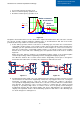
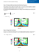
2.2 Modes of Operation
Since the LLC network gain is frequency modulated, the converter can operate in three modes depending on
input voltage and load current conditions, as listed below and shown in Figure 2.4:
0.1 1 10
0
1
2
3
K .2 m, Fx,
(
)
K .3 m, Fx,
(
)
K .5 m, Fx,
(
)
K .7 m, Fx,
(
)
K 1 m, Fx,
(
)
K 5 m, Fx,
(
)
Fx
Capacitive
region
ZCS
Inductive region
ZVS
m=6
Light load
Heavy load