Application Note AN 2012-09 V1.0 September 2012 Resonant LLC Converter: Operation and Design 250W 33Vin 400Vout Design Example Sam Abdel-Rahman Infineon Technologies North America (IFNA) Corp.
Application Note AN 2012-09 Resonant LLC Converter: Operation and Design V1.0 September 2012 Resonant LLC Converter: Operation and Design Sam Abdel-Rahman Published by Infineon Technologies North America 27703 Emperor Blvd, suite 310 Durham, NC 27703 All Rights Reserved.
Application Note AN 2012-09 Resonant LLC Converter: Operation and Design V1.0 September 2012 Table of contents 1 Introduction..................................................................................................................................................4 2 Overview of LLC Resonant Converter.......................................................................................................4 3 Design Steps ................................................................................
Application Note AN 2012-09 Resonant LLC Converter: Operation and Design 1 V1.0 September 2012 Introduction While a resonant LLC converter has several desired features such as high efficiency, low EMI and high power density, the design of a resonant converter is an involved task, and requires more effort for optimization compared to PWM converters. This document aims to simplify this task, and make it easier to optimally design the resonant tank.
Application Note AN 2012-09 Resonant LLC Converter: Operation and Design V1.
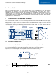
Application Note AN 2012-09 Resonant LLC Converter: Operation and Design V1.0 September 2012 1. At resonant frequency operation, fs=fr. 2. Above resonant frequency operation fs>fr. 3. Below Resonant frequency operation, fs
Application Note AN 2012-09 Resonant LLC Converter: Operation and Design S1 S3 Cr Lr Np D1 Ns S1 D3 S3 Cr Lr + Vo - Lm S2 V1.0 September 2012 S4 D2 Np Ns D1 D3 + Vo - Lm S2 D4 S4 D2 Figure 2.7 D4 Figure 2.8 Table 1 explains the converter modes of operation and shows key waveforms Table 1 At Resonant frequency operation fs=fr. Above resonant frequency operation fs>fr.
Application Note AN 2012-09 Resonant LLC Converter: Operation and Design 3 V1.0 September 2012 Design Steps This section is to explain the impact of design parameters on voltage regulation and efficiency performance, and facilitate the design and selection of such parameters. Our ultimate design objective it to achieve the best performance while reaching the gain requirement for all line and load conditions.
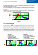
Application Note AN 2012-09 Resonant LLC Converter: Operation and Design V1.0 September 2012 value curve (Q=1) can reach the minimum gain (K=0.8) with less switching frequency increase, but unable to reach the maximum gain (K=1.2). Therefore, a moderate Q value of around 0.5 seems to satisfy the voltage gain requirement in this specific case.
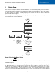
Application Note AN 2012-09 Resonant LLC Converter: Operation and Design V1.0 September 2012 Step 3: Finding the Minimum Normalized Switching Frequency After selecting a value for Qmax and an initial value for m, we need to find the minimum normalized switching frequency that will guarantee inductive operation for the Qmax (max load) condition, this minimum frequency will also guarantee inductive operation for all other loads.
Application Note AN 2012-09 Resonant LLC Converter: Operation and Design V1.0 September 2012 Few iterations are needed in order to reach the optimized design, as shown in the design flow chart in Figure 3.1. If Kmax is not enough, then we have to reduce the m value and repeat steps 3 and 4, in order to gain a higher boost gain. On the other side, If Kmax is higher than what is required; in that case we can increase the m value and repeat steps 3 and 4 in order to gain a better efficiency.
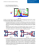
Application Note AN 2012-09 Resonant LLC Converter: Operation and Design V1.0 September 2012 Table 2 Primary Bridge - Half-Bridge compared to Full-Bridge Irms Irms2 Number of FETs Total FETs conduction Np Rpri Transformer primary losses ×2 ×4 ÷2 copper loss ×2 ÷2 ÷2 ×2 *Comparison assumes same FET and same transformer core LLC converters can also be implemented with a full-bridge or a full-wave rectifier circuit on the secondary side, as shown in Figure 4.
Application Note AN 2012-09 Resonant LLC Converter: Operation and Design 5 Design Example 5.1 Application and Specifications V1.0 September 2012 Our design example is applicable to the dc-dc stage of a solar micro inverter, as shown in Figure 5.1, with specifications as listed in Table 4. According to the discussion in section 4, the LLC converter will be implemented with a full-bridge on the primary side and a full-bridge rectifier on the secondary side, same circuit as shown in Figure 2.1.
Application Note AN 2012-09 Resonant LLC Converter: Operation and Design ݀ ܳ(ܭ ௫ , ݉ , ܨ )ฬ ݀ܨ ொ , ୀ.ଷ ೌೣ ୀ.ସ =0 V1.0 September 2012 → ܨ = 0.489 → ݂௦_ = ܨ ∙ ݂ = 48.9 ݇ݖܪ Step 4: Voltage Gain Verification Since the power is derated at lower input voltages as listed in the specifications, we have to calculate the maximum Q value at the minimum input voltage case (ܳ ௫@ ), as follows.
Application Note AN 2012-09 Resonant LLC Converter: Operation and Design 5.3 V1.0 September 2012 Experimental Waveforms and Efficiency The design example was implemented with the specification shown in Table 5 Table 5 Prototype specifications Resonant frequency ݂ 110 kHz Resonant capacitor ܥ 0.94 µF Minimum switching frequency ݂௦_ 50 kHz Transformer Specifications Turns ratio ܰ : ܰ௦ 1:12 Magnetizing inductor ܮ 12.2 µH Leakage (Resonant) inductor ܮ 2.2 µH Figure 5.
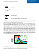
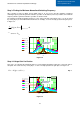
Application Note AN 2012-09 Resonant LLC Converter: Operation and Design V1.0 September 2012 Table 6 Efficency data Output Power (% of 250W) Input Voltage 20% 40% 60% 80% 100% 36V 97.1% ** 97.1%** 97.1% 97.1% 97.1% 33V 96.0% 97.2% 97.6% 97.6% 97.4% 24V 94.5% 96.8% 97.1% 97.0% 18V 94.0% 96.3% 96.2% ** Missing cycle mode / Burst mode operation 98.0% 97.6% 97.4% 96.9% 97.0% Efficiency % 97.6% 97.4% 97.5% 96.5% 96.0% 96.0% Vin= 33V 95.5% Vin= 24V 95.0% Vin= 36V 94.
Application Note AN 2012-09 Resonant LLC Converter: Operation and Design 6 V1.0 September 2012 Schematics and Bill of Material C1 INPUT W1 Jumper INPUT INPUT+ C2 1 2 C3 10uF/100V 10uF/100V D1 1N5819HW-7-F R1 Q1 C7 D2 1N5819HW-7-F R2 SA CON1 400V 2.2nF/500VAC R3 10k Q3 D3 IDH05G65C5 Q2 SC 0 C8 BSC028N06NS 0 BSC028N06NS C5 D4 2.2u/450V IDH05G65C5 C6 2.2u/450V R4 10k Q4 + C4 NC 10uF/100V 10uF/100V PGND INPUT- PBSS4032PT,215 C12 1 2 C13 SW2 + C25 NC C10 2.
Application Note AN 2012-09 Resonant LLC Converter: Operation and Design V1.
Application Note AN 2012 2012-09 Resonant LLC Converter: Operation and Design V1.0 September 2012 Figure 6.2 7 References [1] Infineon Technologies: ICE2HS01G datasheet, High Performance Resonant Mode Controller, V1.1, August 2011. [2] Infineon Technologies: Design Guide for LLC Converter with ICE2HS01G, ICE2HS01G, V1.0, July 2011. [3] Infineon Technologies: 300W W LLC Evaluation Board with LLC controller ICE2HS01G, V1.1, August 2011.