M38517T-ADS Temporary Target Board for M38507ARLSS and M38517RSS User's Manual Rev.1.
Keep safety first in your circuit designs! • Renesas Technology Corporation and Renesas Solutions Corporation put the maximum effort into making semiconductor products better and more reliable, but there is always the possibility that trouble may occur with them. Trouble with semiconductors may lead to personal injury, fire or property damage.
Contents 1. Things to Check When Unpacking ..................................................................................... 4 2. Outline ................................................................................................................................ 4 3. Specifications ..................................................................................................................... 4 4. Setting Up .......................................................................................
1. Things to Check When Unpacking The M38517T-ADS package consists of the following products. When unpacking your package, check to see that all of these components are included. Table 1.1 Package components Content Temporary target board User's manual M38517T-ADS M38517T-ADS User's manual (English/Japanese) * If you find any item missing or faulty, or any suggestion, contact your local distributor. 2.
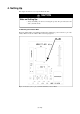
4. Setting Up This chapter describes how to set up the M38517T-ADS. CAUTION Note on Setting Up: • Always shut OFF power before connecting this product. The power ON state could destroy internal circuits. 4.1 Mounting an Emulator MCU Mount an emulator MCU on the M38517T-ADS. After checking the position of the No. 1 pin of the emulator MCU, mount the emulator MCU referencing Figure 4.1. Figure 4.1 Position of No.
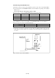
4.2 Connecting to the Emulation Pod (1) Insert the connector on the tip of the emulation pod probe to the socket on the emulator MCU. (2) Connect the cables of the M38000TL2-PSW2 as shown in Table 4.1 depending on the emulator MCU you use. Do not connect the Vcc cable (yellow) to pin Vcc (TP1). Table 4.
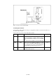
Figure 4.3 Connecting the M38517RSS 4.3 Setting the Switches Set the switches SW1 to SW3 according to your applications. Table 4.3 describes the functions of the switches SW1 to SW3. Table 4.3 Functions of the switches SW1, SW2 and SW3 No. Name Function Factory-setting SW1 PORT/XCIN Allows you to choose whether to supply the sub-clock signals (32.768 kHz) to the MCU's XCIN pin (pin 16). To use pin P21/XCIN as an I/O port, choose the PORT side. To use the sub-clock signals, choose the XCIN side.
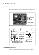
5. Oscillator Circuit 5.1 Oscillator Circuit Board The M38517T-ADS has a built-in oscillator circuit board on which a 4.0MHz oscillator is mounted. Figure 5.1 shows an external view of the OSC-2 oscillator circuit board (bare board) and where connector pins are located. Figure 5.2 shows the circuitry of the OSC-2 oscillator circuit board (bare board). Use the number of oscillator circuits recommended by the oscillator manufacturer.
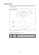
6. Reset Circuit Figure 6.1 shows the reset circuit and its waveform. In this product, reset is cleared in about 100 ms from the instant Vcc passes about 2.1 V after having started from 0 V. When Vcc drops down to about 2.1 V, reset turns effective. Detected power voltage (V) About 1.25 x (R3 + R4) / R4 Figure 6.1 Reset circuit and its waveform By using the switch SW4, the MCU can be reset manually. Table 6.1 Function of SW4 (reset switch) No. Name SW4 RESET Function This is the reset switch.
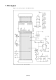
7. Pin Layout Figure 7.1 shows the pin layout of the M38517T-ADS. Figure 7.
M38517T-ADS User's Manual Rev.1.