REJ10B0186-0100 SuperHTM Family E10A Emulator Additional Document for User’s Manual Specific Guide for the SH7710 E10A Emulator Renesas Microcomputer Development Environment System SuperH Family / SH7700 Series SH7710 E10A HS7710KCM02HE Rev.1.00 Revision Date: Mar.
Keep safety first in your circuit designs! 1. Renesas Technology Corp. puts the maximum effort into making semiconductor products better and more reliable, but there is always the possibility that trouble may occur with them. Trouble with semiconductors may lead to personal injury, fire or property damage.
Contents Section 1 Connecting the Emulator with the User System ................................1 1.1 1.2 1.3 1.4 1.5 Components of the Emulator ............................................................................................ 1 Connecting the Emulator with the User System ............................................................... 3 Installing the H-UDI Port Connector on the User System ................................................ 4 Pin Assignments of the H-UDI Port Connector ..........
ii
Section 1 Connecting the Emulator with the User System 1.1 Components of the Emulator The SH7710 E10A emulator supports the SH7710. Table 1.1 lists the components of the emulator. Table 1.1 Components of the Emulator (HS7710KCM01H, HS7710KCM02H, HS7710KCI01H, or HS7710KCI02H) Classification Component Hardware Card emulator Appearance Insert PC Card Emulator H-UDI Micro Computer Development System PC Card Quantity 1 HITACHI (PCMCIA) Remarks HS7710KCM01H (PCMCIA: 14-pin type): Depth: 85.
Table 1.
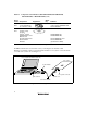
1.2 Connecting the Emulator with the User System To connect the E10A emulator (hereinafter referred to as the emulator), the H-UDI port connector must be installed on the user system to connect the user system interface cable. When designing the user system, refer to an example of recommended connection between the connector and the MPU shown in this manual. In addition, read the E10A emulator user's manual and hardware manual for the related device. Table 1.
1.3 Installing the H-UDI Port Connector on the User System Table 1.3 shows the recommended H-UDI port connectors for the emulator. Table 1.3 Recommended H-UDI Port Connectors Connector Type Number Manufacturer Specifications 36-pin connector DX10M-36S Hirose Electric Co., Ltd. Screw type DX10M-36SE, DX10G1M-36SE 14-pin connector 2514-6002 Lock-pin type Minnesota Mining & Manufacturing Ltd.
Pin No. Signal Input/ SH7710 Output *1 Pin No. Note Pin No. Signal 1 AUDCK Output 19 TMS 2 GND 20 GND 3 AUDATA0 21*2 /TRST 4 GND 5 AUDATA1 6 GND 7 AUDATA2 8 GND 9 AUDATA3 10 GND 11*2 /AUDSYNC 12 GND 30 13 NC 31*2 /RESETP 14 GND 32 15 NC 33*3 GND 16 GND 34 GND 17 TCK 35 NC 18 GND 36 GND Output 205 213 Input/ Output *1 SH7710 Pin No.
SH7710 Pin No. Signal Input/ Output*1 1 TCK Input 202 2 /TRST Input 201 3 TDO Output 200 4 /ASEBRKAK Output 203 5 TMS Input 199 6 TDI Input 198 7 /RESETP I/O 215 8 N.C. 9 (GND) *5 11 UVCC *4 Output 10, 12, GND *3 Output Pin No. *2 *2 *2 Note User reset and 13 14 GND Notes: 1. Input to or output from the user system. 2. The slash (/) means that the signal is active-low. 3.
1.5 Recommended Circuit between the H-UDI Port Connector and the MPU 1.5.1 Recommended Circuit (36-Pin Type) Figure 1.5 shows a recommended circuit between the H-UDI port connector (36 pins) and the MPU. Notes: 1. Do not connect anything to the N.C. pins of the H-UDI port connector. 2. The processing of the /ASEMD0 pin differs depending on whether the emulator is used or not. As the emulator does not control this pin, it must be controlled by a switch on the board.
E10A CPU 3.3 V 4.7 kΩ TMS, TRST Diode equivalent to 1SS106* Note: Schottky-barrier diode Figure 1.4 Countermeasure against the Leakage Current in the Emulator The result above differs depending on the circuit and can only be used as a reference. 7. The resistance values shown in figure 1.5 are recommended. 8. For the pin processing in cases where the emulator is not used, refer to the hardware manual of the related device. 9.
VccQ (3.3 V) H-UDI port connector (36-pin type) 2 4 6 8 10 12 14 16 18 20 22 24 26 28 30 32 34 36 GND GND GND GND GND AUDCK AUDATA0 AUDATA1 AUDATA2 AUDATA3 GND AUDSYNC GND N.C. GND N.C. GND TCK GND GND GND GND TMS TRST TDI TDO GND ASEBRKAK GND N.C. GND RESET GND GND GND N.C. VccQ (3.3 V) 4.7 kΩ SH7710 4.
1.5.2 Recommended Circuit (14-Pin Type) Figure 1.7 shows a recommended circuit between the H-UDI port connector and the MPU. Notes: 1. Do not connect anything to the N.C. pins of the H-UDI port connector. 10 2. The processing of the /ASEMD0 pin differs depending on whether the emulator is used or not. As the emulator does not control this pin, it must be controlled by a switch on the board. (1) When the emulator is used: /ASEMD0 = low (2) When the emulator is not used: /ASEMD0 = high 3.
E10A CPU 3.3 V 4.7 kΩ TMS, TRST Diode equivalent to 1SS106* Note: Schottky-barrier diode Figure 1.6 Countermeasure against the Leakage Current in the Emulator The result above differs depending on the circuit and can only be used as a reference. 7. The resistance values shown in figure 1.7 are recommended. 8. For the pin processing in cases where the emulator is not used, refer to the hardware manual of the related device. VccQ (3.3 V) VccQ (3.3 V) 4.
12
Section 2 Specifications of the SH7710 E10A Emulator’s Software 2.1 Differences between the SH7710 and the Emulator 1. When the emulator system is initiated, it initializes the general registers and part of the control registers as shown in table 2.1. The initial values of the actual SH7710 registers are undefined. Table 2.
3. Low-Power States (Sleep, Software Standby, and Module Standby) For low-power consumption, the SH7710 has sleep, software standby, and module standby states. The sleep, software standby, and module standby states are switched using the SLEEP instruction. When the emulator is used, only the sleep state can be cleared with either the normal clearing function or with the [STOP] button, and a break will occur. Note: The memory must not be accessed or modified in sleep state. 4.
8. Cache Operation during User Program Break When cache is enabled, the emulator accesses the memory by the following methods: At memory write: Writes through the cache, then writes to the memory. At memory read: Does not change the cache write mode that has been set. Therefore, when memory read or write is performed during user program break, the cache state will be changed. 9.
Table 2.2 Watchdog Timer Register Register Name Usage Register WTCSR(W) Write Watchdog timer control/status register WTCNT(W) Write Watchdog timer counter WTCSR(R) Read Watchdog timer control/status register WTCNT(R) Read Watchdog timer counter The watchdog timer operates only when the user program is executed. Do not change the value of the frequency change register in the [IO] window or [Memory] window. The internal I/O registers can be accessed from the [IO] window.
2.2 Specific Functions for the SH7710 E10A Emulator 2.2.1 Emulator Driver Selection Table 2.3 shows drivers which are selected in the [E10A Driver Details] dialog box. Table 2.
2.2.2 Break Condition Functions In addition to BREAKPOINT functions, the emulator has Break Condition functions. Three types of conditions can be set under Break Condition 1, 2, 3. Table 2.4 lists these conditions of Break Condition. Table 2.4 Types of Break Conditions Break Condition Type Description Address bus condition (Address) Breaks when the SH7710 address bus value or the program counter value matches the specified value.
Table 2.5 lists the combinations of conditions that can be set under Break Condition 1, 2, 3. Table 2.
AUD Trace Functions: This function is operational when the AUD pin of the device is connected to the emulator. Table 2.8 shows the AUD trace acquisition mode that can be set in each trace function. Table 2.8 AUD Trace Acquisition Mode Type Mode Description Continuous trace occurs Realtime trace When the next branch occurs while the trace information is being output, the trace information being output is output but the next trace information is not output.
To set the AUD trace acquisition mode, click the [Trace] window with the right mouse button and select [Setting] from the pop-up menu to display the [Acquisition] dialog box. The AUD trace acquisition mode can be set in the [AUD mode1] or [AUD mode2] group box in the [Trace mode] page of the [Acquisition] dialog box. Figure 2.1 [Trace mode] Page When the AUD trace function is used, select the [AUD function] radio button in the [Trace type] group box of the [Trace mode] page.
(a) Branch Trace Function The branch source and destination addresses and their source lines are displayed. Branch trace can be acquired by selecting the [Branch trace] check box in the [AUD function] group box of the [Trace mode] page. The branch type can be selected in the [AUD Branch trace] page. Figure 2.2 [AUD Branch trace] Page (b) Window Trace Function Memory access in the specified range can be acquired by trace. Two memory ranges can be specified for channels A and B.
Figure 2.3 [Window trace] Page Notes: 1. When the [L-bus] or [I-bus] radio button is selected, the following bus cycles will be traced. • L-bus: A bus cycle generated by the CPU is acquired. A bus cycle is also acquired when the cache has been hit. • I-bus: A bus cycle generated by the CPU or DMA is acquired. A bus cycle is not acquired when the cache has been hit. The address information acquired by the Ibus is 28 bits and the upper 4 bits are displayed as ‘*’.
(c) Software Trace Function Note: This function can be supported with SHC/C++ compiler (manufactured by Renesas Technology Corp.; including OEM and bundle products) V7.0 or later. When a specific instruction is executed, the PC value at execution and the contents of one general register are acquired by trace. Describe the Trace(x) function (x is a variable name) to be compiled and linked beforehand. For details, refer to the SHC manual.
9. For the AUD non-realtime trace, the written access may be executed again. If this is a problem on the user system, do not use the non-realtime trace. Internal Trace Function: This function is activated by selecting the [Internal trace] radio button in the [Trace type] group box of the [Trace mode] page. This function traces and displays the branch instructions. The branch source address and branch destination address for the eight latest branch instructions are displayed. See figure 2.
An area that can be only read by MMU 3. During step operation, a BREAKPOINT is disabled. 4. Conditions set at Break Condition 2 are disabled when an instruction to which a BREAKPOINT has been set is executed. Do not set a BREAKPOINT to an instruction in which Break Condition 2 is satisfied. 5. When execution resumes from the address where a BREAKPOINT is specified, single-step operation is performed at the address before execution resumes. Therefore, realtime operation cannot be performed. 6.
value after setting. When no ASID value is specified, the BREAKPOINT is set to a virtual address corresponding to the ASID value at command input. 12. An address (physical address) to which a BREAKPOINT is set is determined when the BREAKPOINT is set. Accordingly, even if the VP_MAP table is modified after BREAKPOINT setting, the BREAKPOINT address remains unchanged.
2.2.7 Note on Setting the UBC_MODE Command In the [Configuration] dialog box, if [User] is set while the [UBC mode] list box has been set, the STEP-type commands that use Break Condition 2 for implementation cannot be used. 2.2.8 Performance Measurement Function The SH7710 E10A emulator supports the performance measurement function. 1. Setting the performance measurement conditions To set the performance measurement conditions, use the [Performance Analysis] dialog box and the PERFORMANCE_SET command.
Figure 2.4 [Performance Analysis] Dialog Box (b) Measurement range One of the following ranges can be specified. This depends on the item selected for [Mode] in the [Performance Analysis] dialog box. 1. From the start to the end of the user program execution (When Normal Break is selected for [Mode]) 2. From the satisfaction of the condition set in Break Condition 1 to the satisfaction of the condition set in Break Condition 2 (When Break condition 1->2 is selected for [Mode]) 3.
Notes: 1. When the second and third ranges are specified, execute the user program after the measurement start condition is set to Break Condition 1 (or Break Condition 2) and the measurement end condition to Break Condition 2 (or Break Condition 1). 2. Step operation is not possible when Break condition 1->2 or Break condition 2->1 is selected for the PERFORMANCE_SET command or in [Mode] of the [Performance Analysis] dialog box. 3.
Table 2.10 Measurement Item Selected Name Option Disabled None Elapsed time AC Number of execution states VS Branch instruction counts BT Number of execution instructions I DSP-instruction execution counts DI (Devices incorporating the DSP function can only be measured.) Instruction/data conflict cycle MAC Other conflict cycles than instruction/data OC Exception/interrupt counts EA Data-TLB miss cycle MTS (Devices incorporating the MMU function can only be measured.
Table 2.
Note: If a performance counter overflows as a result of measurement, “********” will be displayed. 3. Initializing the measured result To initialize the measured result, select [Initialize] from the popup menu in the [Performance Analysis] window or specify INIT with the PERFORMANCE_ANALYSIS command.
34
SuperH Family E10A Emulator Additional Document for User's Manual Specific Guide for the SH7710 E10A Emulator Publication Date: Rev.1.00, March 1, 2005 Published by: Sales Strategic Planning Div. Renesas Technology Corp. Edited by: Technical Documentation & Information Department Renesas Kodaira Semiconductor Co., Ltd. 2005. Renesas Technology Corp., All rights reserved. Printed in Japan.
Sales Strategic Planning Div. Nippon Bldg., 2-6-2, Ohte-machi, Chiyoda-ku, Tokyo 100-0004, Japan RENESAS SALES OFFICES http://www.renesas.com Refer to "http://www.renesas.com/en/network" for the latest and detailed information. Renesas Technology America, Inc. 450 Holger Way, San Jose, CA 95134-1368, U.S.A Tel: <1> (408) 382-7500, Fax: <1> (408) 382-7501 Renesas Technology Europe Limited Dukes Meadow, Millboard Road, Bourne End, Buckinghamshire, SL8 5FH, U.K.
SuperH Family E10A Emulator Additional Document for User’s Manual Specific Guide for the SH7710 E10A Emulator