
User`s manual


20
11. Loading Sessions
Information in [JTAG clock] of the [Configuration] dialog box cannot be recovered by loading
sessions. Thus the TCK value will be as follows:
• When HS0005KCU01H or HS0005KCU02H is used: TCK = 1.25 MHz
12. [IO] Window
• Display and modification
For registers with different read and write access sizes, there are two registers to be
separately used for read and write operations.
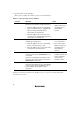
Table 2.7 Registers with Different Access Sizes
Register Name Usage Register
WTCSR(W) Write Watchdog timer control/status register
WTCNT(W) Write Watchdog timer counter
WTCSR(R) Read Watchdog timer control/status register
WTCNT(R) Read Watchdog timer counter
WRCSR(W) Write Watchdog reset control/status register
WRCSR(R) Read Watchdog reset control/status register
STRMDIN0_1(R) Read CD-ROM decoder stream data input register 0/1
STRMDIN2_3(R) Read CD-ROM decoder stream data input register 2/3
STRMDIN0_3(W) Write CD-ROM decoder stream data input register 0/1/2/3
• Customization of the I/O-register definition file
The internal I/O registers can be accessed from the [IO] window. However, note the
following when accessing the SDMR register of the bus-state controller. Before accessing
the SDMR register, specify addresses to be accessed in the I/O-register definition file
(SH7201.IO, SH7261x.IO, or (MCU name).IO) and then activate the High-performance
Embedded Workshop. After the I/O-register definition file is created, the MCU’s
specifications may be changed. If each I/O register in the I/O-register definition file differs
from addresses described in the hardware manual, change the I/O-register definition file
according to the description in the hardware manual. The I/O-register definition file can be
customized depending on its format. Note that, however, the emulator does not support the
bit-field function.
• Verify
In the [IO] window, the verify function of the input value is disabled.