
User`s manual

Section 2 Connecting the Emulator to the User System
Rev. 3.00 Oct. 17, 2008 Page 24 of 66
REJ10J1662-0300
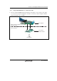
SH7286
1
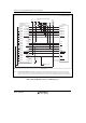
AUDATA0
AUDATA2
AUDATA1
AUDATA3
TCK
TMS
AUDSYNC
N.C.
N.C.
RES
TDI
TDO
TRST
ASEBRKAK
/ASEBRK
UVCC
GND
Reset signal
GND
GND
GND
(GND)
GND
GND
GND
GND
GND
GND
GND
GND
GND
GND
GND
GND
GND
GND
3
5
7
9
11
13
15
17
19
21
23
25
27
29
31
33
35
2
4
6
8
12
10
14
16
18
20
22
24
26
28
30
32
34
36
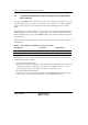
AUDATA0
AUDATA2
AUDATA1
AUDATA3
TCK
RES
TMS
TDO
TDI
TRST
ASEBRKAK
/ASEBRK *
AUDCK
AUDSYNC
AUDCK
N.C.
VCC
ASEMD0
VCC
VCC
VCC
1 kΩ
All pulled-up at 4.7 kΩ or more
VCC = I/O power supply
User system
Note:
The ASEBRKAK#/ASEBRK# pin (I/O pin) is multiplexed with the FWE pin (input pin). For the pin processing when the
emulator is used and the user system is independently in operation, pins must be pulled up at 4.7 kΩ or more or pulled
down at 100 kΩ. For the pin processing when the emulator is not used, refer to the hardware manual of the related MCU.
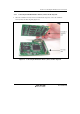
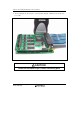
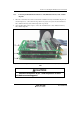
H-UDI port connector
(36-pin type)
Figure 2.12 Recommended Circuit for Connection between the H-UDI Port Connector and
MCU when the Emulator is in Use (36-Pin Type) (1)