
User`s manual


SuperH Family E10A-USB Emulator Section 6 Tutorial
R20UT0870EJ1000 Rev. 10.00 Page 255 of 292
Aug 10, 2012
The write and erase modules must not contain SLEEP, DIVS, DIVU, or REBANK
instructions.
FPU exceptions must not occur within the write and erase modules.
The module interface must be as follows so that the information required for flash memory
access is passed correctly.
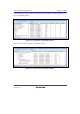
Table 6.3 Module Interface
Module Name Argument Return Value
Write module R4(L): Write address
R5(L): Access size
0x4220 = byte,
0x5720 = word,
0x4C20 = longword
R6(L): Write data
R0(L): End code
Normal end = 0,
Abnormal end = other than 0
Erase module R4(L): Access size
0x4220 = byte,
0x5720 = word,
0x4C20 = longword
None
Note: The (L) means the longword size.
Note: Write module: The write data for the access size is set to the R6 register. When the access
size is word or byte, 0 is set to the upper bits of the R6 register.