
User`s manual


Functional Overview
2.3.3 SRAM
Rev.1.01
Jan 31, 2008
2-9
REJ10J1262-0101
2
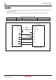
Figure 2.3.4 shows the example of SRAM read timing when the bus clock is 40MHz and Figure 2.3.5 shows the
example of SRAM write timing when the bus clock is 40MHz.
tRSD
Th T1 Tw1 Tw2 Tw3 T2 Tf
CKIO
tcyc
(25ns)
A20-A1
CS4
RD
D15-D0
tAD1
tCSD1
tRDS1
tRSD
tRC
tCLZ
tOE
tOLZ
tCHZ1
tOH
WEn
tWED2
RD/WR
tAD1
tBHZ
tOHZ
tAA
tBA
tACS1
tRDH1
(A19-A0)
(CS1)
(UB,LB)
(WE)
(OE)
Figure 2.3.4 Example of SRAM Read Timing
Th T1 Tw1 Tw2 Tw3 T2 Tf
CKIO
tcyc
(25ns)
A20-A1
CS4
D15-D0
tAD1
tCSD1
tWDD1
tWC
tDW
tWP
tWR
tDH
WEn
tWED2
RD/WR
tAD1
tOW
tBW
tCW
tWDH1
(CS1)
(A19-A0)
(UB,LB)
(WE)
tRWD1
tRWD1
tAS
tAW
Figure 2.3.5 Example of SRAM Write Timing