
User`s manual


Functional Overview
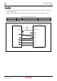
2.3.3 SRAM
Rev.1.01
Jan 31, 2008
2-8
REJ10J1262-0101
2
Table2.3.4 lists the setting example of bus state controller when the bus clock of SH7211 is operating at 40 MHz.
Table2.3.4 Setting Examples of Bus State Controller (CS4 Space)
User Area Target Device SDRAM Controller Settings
CS4 R1LV1616RSA-7S CS4 Space Bus Control Register : CS4BCR
Initial value : H’36DB 0400, Recommended value : H'1659 3400
•
Idle cycles between write-read cycles and write-write cycles
IWW[2:0] = 001 ; 1
idle cycle inserted
•
Idle cycles for another space read-write
IWRWD[2:0] = 011 ; 4
idle cycle inserted
•
Idle cycles for read-write in same space
IWRWS[2:0] = 001 ; 1
idle cycle inserted
•
Idle cycles for another space read-read
IWRRD[2:0] = 011 ; 4
idle cycle inserted
•
Idle cycles for read-read in same space
IWRRS[2:0] = 001 ; 1
idle cycle inserted
• Specify memory type
TYPE[2:0] = 011 ; Byte selection SRAM
• Specify data bus type
BSZ[1:0] = 10 ; 16 bit bus width
CS4 Space Wait Control Register : CS4WCR
Initial value: H’0000 0500, Recommended value: H’
•
Byte access selection for byte-selection SRAM
BAS = 1 ; Asserts the WEn during the read/write access cycle and
asserts the RDWR at the write timing.
•
Number of write access wait cycles
WW[2:0] = 000 ;
Same number of cycles as the number of read
access wait
•
Number of delay cycles from address, CS4 assertion to RD, WEn
assertion
SW[1:0] = 01 ; 1.5 cycles
• Number of read access wait cycles
WR[3:0] = 0011 ; 3 cycles
•
External wait mask specification
WM =1 ;
External wait is ignored
•
Number of delay cycles from RD, WEn negation to address, CS4
negation
HW[1:0] = 01;1.5 cycles