REJ10J1262-0101 SH7211 CPU Board M3A-HS11 32 User's Manual Renesas 32-Bit RISC Microcomputers SuperH RISCengine Family / SH7211 Group TM Rev. 1.
Notes regarding these materials 1. This document is provided for reference purposes only so that Renesas customers may select the appropriate Renesas products for their use. Renesas neither makes warranties or representations with respect to the accuracy or completeness of the information contained in this document nor grants any license to any intellectual property rights or any other rights of Renesas or any third party with respect to the information in this document. 2.
Table of Contents Chapter1 Overview .............................................................................................................................. 1-1 1.1 Overview .................................................................................................................................................................... 1-2 1.2 Configuration .................................................................................................................................................
Appendix..............................................................................................................................................A-1 M3A-HS11 SCHEMATICS Rev. 1.
Chapter1Overview Chapter1 Overview 1-1
Overview 1 1.1 Overview 1.1 Overview The M3A-HS11 is the CPU board designed for users to evaluate the functionality and performance of the SH7211 group of Renesas Technology original microcomputers, as well as develop and evaluate the application software for this group of microcomputers.
Overview 1 1.3 External Specifications 1.3 External Specifications Table1.3.1 lists external specifications of M3A-HS11. Table1.3.1 External Specifications of M3A-HS11 No. Item Content SH7211 1 CPU • Input(XIN) Clock : 10MHz • CPU Clock : 160MHz,max • Bus Clock : 40MHz,max • On-chip memory Flash Memory : 512KB RAM : 32KB • SDRAM : 16-Mbyte EDS1216AATA-75E 1pc. (16-bit bus width) 2 Memory • SRAM : 2-Mbyte (SRAM with byte selection) R1LV1616RSA7S 1pc.
Overview 1 1.4 External View 1.4 External View Figure1.4.1 shows the external view of M3A-HS11. Figure1.4.1 External View of M3A-HS11 Rev.1.
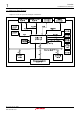
Overview 1 1.5 M3A-HS11 Block Diagram 1.5 M3A-HS11 Block Diagram Figure1.5.1 shows the system block diagram of M3A-HS11. Figure1.5.1 System Block Diagram of M3A-HS11 Rev.1.
Overview 1 1.6 M3A-HS11 Board Overview 1.6 M3A-HS11 Board Overview Figure1.6.1 shows the M3A-HS11 board overview.
Overview 1 1.6 M3A-HS11 Board Overview Table1.6.1 lists main components mounted in the M3A-HS11. Table1.6.1 Main Components Mounted in the M3A-HS11 Symbol Parts Name Remarks Recommended Parts Number for Not-Mounted Components U1 CPU SH7211 (Renesas) U2 Clock Buffer Not mounted U3 SRAM R1LV1616RSA7S U4 EEPROM HN58X24128FPIE U5 SDRAM EDS1216AATA-75E U6 RS-232C Driver SP3232ECA(Sipex) U7 3.3V Voltage Regulator LMS1587CSX-ADJ(NS) U8 1.
Overview 1 1.7 M3A-HS11 Memory Mapping 1.7 M3A-HS11 Memory Mapping Figure1.7.1, Figure1.7.2 and Figure1.7.3 show the SH7211 memory mapping examples in the M3A-HS11 on each MCU mode.
Overview 1 1.
Overview 1 1.
Overview 1 1.8 Absolute Maximum Ratings 1.8 Absolute Maximum Ratings Table1.8.1 lists the absolute maximum ratings of M3A-HS11. Table1.8.1 Absolute Maximum Ratings of M3A-HS11 Symbol Parameter Rated Value Remarks 5VCC 5V System Power Supply Voltage -0.3V to 6.0V Relative to VSS 3VCC 3.3V System Power Supply Voltage -0.3V to 4.6V Relative to VSS 1.5VCC 1.5V System Power Supply Voltage -0.3V to 2.3V Relative to VSS Operating Ambient Temperature -10°C to 55°C No dewdrops allowed.
Overview 1 1.8 Absolute Maximum Ratings * This is a blank page * Rev.1.
Chapter2Functional Overview Chapter2 Functional Overview 2-1
2 Functional Overview 2.1 Functional Overview 2.1 Functional Overview The M3A-HS11 is the SH7211 CPU board that has the functions listed in Table2.1.1. Table2.1.1 lists the functional modules of M3A-HS11. Table2.1.1 Functional Modules of M3A-HS11 Section 2.2 Function CPU Content SH7211 • Input(XIN) Clock: 10 MHz • CPU Clock: Maximum 160 MHz, • Bus Clock: Maximum 40 MHz • On-Chip Memory - Flash Memory: 512 KB - RAM : 32 KB 2.3 Memory • SDRAM: 16-Mbyte EDS1216AATA-75E 1pc.
2 Functional Overview 2.2 CPU 2.2 CPU The M3A-HS11 contains the 32-bit RISC microcomputer SH7211 that operates with a maximum 160MHz of CPU clock frequency. The SH7211 includes 512-Kbyte flash memory, and 32-Kbyte RAM, making it useful in a wide range of applications from data processing to equipment control. The M3A-HS11 can be operated with a maximum 160MHz of CPU clock frequency (external bus 40MHz, max) using a 10MHz input clock. Figure 2.2.1 shows the SH7211 block diagram in the M3A-HS11.
2 Functional Overview 2.3 Memory 2.3 Memory 2.3.1 SH7211 On-Chip Memory The SH7211 includes 512-Kbyte flash memory and 32-Kbyte RAM. 2.3.2 SDRAM The M3A-HS11 mounts 16MB SDRAM as standard equipment. The SDRAM is controlled by the bus state controller built into SH7211. Table2.3.1 lists the SDRAM specifications used in M3A-HS11. Figure 2.3.1 shows the block diagram of SDRAM connection. Table2.3.
2 Functional Overview 2.3 Memory Table 2.3.2 lists the setting examples of bus state controller when the SH7211 bus clock is operating at 40 MHz. Table 2.3.
Functional Overview 2 2.3 Memory Figure 2.3.2 shows an example of SDRAM single read/write timing for operation that the SH7211 bus clock is operating at 40 MHz.
2 Functional Overview 2.3.3 SRAM 2.3.3 SRAM The M3A-HS11 includes the 2-Mbyte SRAM as standard equipment. The SRAM is controlled by the bus state controller included in SH7211. Table2.3.3 lists the specification outline of SRAM. Figure 2.3.3 shows the block diagram of SH7211 and SRAM. Table2.3.3 SRAM Specification Outline Part Number Bus Size Capacity Package R1LV1616RSA-7S 16-bit 2-Mbyte (16-bit × 1M word × 1 pc.
2 Functional Overview 2.3.3 SRAM Table2.3.4 lists the setting example of bus state controller when the bus clock of SH7211 is operating at 40 MHz. Table2.3.
2 Functional Overview 2.3.3 SRAM Figure 2.3.4 shows the example of SRAM read timing when the bus clock is 40MHz and Figure 2.3.5 shows the example of SRAM write timing when the bus clock is 40MHz. tcyc (25ns) Th T1 Tw1 Tw2 Tw3 T2 Tf CKIO tRC tAD1 tAD1 tAA A20-A1 (A19-A0) tCHZ1 tCSD1 CS4 tACS1 (CS1) tWED2 tBHZ WEn tBA (UB,LB) RD/WR (WE) tRSD tRSD tOE RD (OE) tOHZ tOLZ tCLZ tOH tRDS1 tRDH1 D15-D0 Figure 2.3.
2 Functional Overview 2.3.4 EEPROM 2.3.4 EEPROM The M3A-HS11 includes the 128k-bit EEPROM as standard equipment. The EEPROM is controlled by the I2C bus interface included in SH7211. Table 2.3.5 lists the specification outline of EEPROM. Figure 2.3.6 shows the connection circuit block diagram of SH7211 and EEPROM. Table 2.3.
2 Functional Overview 2.4 Serial Port Interface 2.4 Serial Port Interface In the M3A-HS11, the SCI channel 1 of SH7211 is connected to the serial port connector (J3). Figure 2.4.1 shows the block diagram of serial port interface in the M3A-HS11. SH7211 Serial Port Connector (J3) RS-232C Driver N C PA24/RXD1 PA25/TXD1 1 2 3 4 DCD RxD TxD DTR GN 5 GND D 6 DSR 7 RTS 8 CTS N 9 RI C Figure 2.4.1 Block Diagram of Serial Port Interface Rev.1.
2 Functional Overview 2.5 I/O Ports 2.5 I/O Ports In the M3A-HS11, all of the SH7211's I/O ports are connected to the extension bus connector. Some I/O ports are connected to DIP switches and LEDs of the M3A-HS11 board. Users are free to use these ports. Figure 2.5.1 shows the block diagram of DIP Switch and LEDs in the M3A-HS11. Table 2.5.1 lists the functions of the SH7211 I/O ports in the M3A-HS11.
2 Functional Overview 2.5 I/O Ports Table 2.5.
2 Functional Overview 2.6 Power Supply Circuit 2.6 Power Supply Circuit In the M3A-HS11, the 5V power supply is input to the board and it generates 3.3V and 1.5V by using a regulator. The used regulator uses an output voltage-controlled type so that a desired voltage value can be generated by changing the resistance. Figure 2.6.1 shows the block diagram of power supply circuit in the M3A-HS11.
2 Functional Overview 2.7 Clock Module 2.7 Clock Module The clock module in the M3A-HS11 consists of the following two blocks: • • Output from a oscillator connected to EXTAL of the SH7211 Ceramic resonator connected to EXTAL and XTAL The M3A-HS11 has a 10MHz oscillator connected to it as standard specification. System clock output (PB3/CKIO) of SH7211 is connected to an extension connector with dumping resistor.
2 Functional Overview 2.8 Reset Module 2.8 Reset Module This circuit controls the reset signal of SH7211 mounted on the M3A-HS11. Figure 2.8.1 shows the block diagram of reset module in the M3A-HS11. R1LV1616RSA-7S Reset IC Output Delay Time : td = 0.34 × Cd(pF) = 34ms Reset IC Output Detection Voltage : Ra=10KΩ,Rb=10KΩ Vs = 1.25 × (Ra+Rb)/Rb = 2.5V CS2 Extension Connector 3Vcc 3Vcc RESET Ra Rb M51957BP SH7211 Input RES Output Delay Capacitance Cd 0.1uF Reset Switch (SW2) Figure 2.8.
2 Functional Overview 2.10 E10A-USB Interface 2.10 E10A-USB Interface The M3A-HS11 has the H-UDI connectors (14-pin and 36-pin) to connect with E10A-USB. Figure 2.10.1 shows the block diagram of E10A-USB interface. VccQ VccQ VccQ H-UDI Connector (36-pin) 2 4 6 8 10 GND AUDCK GND AUDATA0 GND AUDATA1 GND AUDATA2 GND 12 GND 14 GND 16 GND 18 GND 20 GND 22 (GND) 24 GND 26 GND 28 GND 30 GND 32 GND 34 GND 36 GND AUDATA3 AUDSYNC N.C. N.C. TCK TMS TRST TDI TDO ASEBRKAK/ASEBRK UVCC RES GND N.C.
2 Functional Overview 2.10 E10A-USB Interface This is a blank page Rev.1.
Chapter 3 Operational Specifications Chapter 3 Operational Specifications 3-1
Operational Specifications 3 3.1 M3A-HS11 Connectors Outline 3.1 M3A-HS11 Connectors Outline Figure 3.1.1 shows M3A-HS11 connector assignments.
Operational Specifications 3 3.1.1 H-UDI Connector (J1, J2) 3.1.1 H-UDI Connector (J1, J2) The M3A-HS11 includes a 36-pin H-UDI (J1) connector and 14-pin H-UDI (J2) connector for a connection to the E10A-USB emulator. Figure 3.1.2 shows a pin assignment of H-UDI (J1) connector. 35 1 36 2 Top View of the Component Side Board Edge Side View Board Edge Figure 3.1.2 Pin Assignment of H-UDI(J1) Connector Table 3.1.1 lists pin assignments of H-UDI connector (J1). Table 3.1.
Operational Specifications 3 3.1.1 H-UDI Connector (J1, J2) Figure 3.1.3 shows a pin assignment of H-UDI (J2) connector. 7 6 5 4 3 2 1 14 13 12 11 10 9 8 Board Edge Top View of the Component Side J2 Side View Board Edge Figure 3.1.3 Pin Assignment of H-UDI (J2) Connector Table 3.1.2 lists pin assignments of H-UDI (J2) connector. Table 3.1.
Operational Specifications 3 3.1.2 Serial Port Connector (J3) 3.1.2 Serial Port Connector (J3) The M3A-HS11 includes a serial port connector (J3). Figure3.1.4 shows a pin assignment of serial port connector. 1 6 5 9 Board Edge Top View of the Component Side 1 6 5 9 Board Edge Side View Figure3.1.4 Pin Assignment of Serial Port Connector (J3) Table 3.1.3 lists pin assignments of serial port connector. Table 3.1.
Operational Specifications 3 3.1.3 Power Supply Connector (J4) 3.1.3 Power Supply Connector (J4) The M3A-HS11 includes the power supply connector pin for the SH7211. Figure 3.1.5 shows a pin assignment of power supply connector. GND +5V 1 2 1 2 Top View of the Component Side Board Edge Side View Board Edge Figure 3.1.5 Pin Assignment of Power Supply Connector (J4) Table 3.1.4 lists a pin assignment of power supply connector for M3A-HS11. Table 3.1.
Operational Specifications 3 3.1.4 External Power Supply Connector for SH7211 (J5, J6) 3.1.4 External Power Supply Connector for SH7211 (J5, J6) The M3A-HS11 includes the external power supply connector pins to supply the power source of 3.3V and 1.5V externally. When the power is supplied by using this connector, set the power select jumper (JP1 and JP2) to “2-3”. Figure 3.1.6 shows a pin assignment of power supply connector. Top View of the Component Side J5 1 1.5V 3.
Operational Specifications 3 3.1.5 A/D, D/A Connector (J7) 3.1.5 A/D, D/A Connector (J7) The M3A-HS11 includes the A/D and D/A connector pins which the A/D and D/A pins of SH7211 are connected. When the voltages of AVCC and AVREF are supplied through this connector, remove the AVCC select jumper (JP3) and AVREF select jumper (JP4). Figure3.1.7 shows a pin assignment of A/D and D/A connectors. Table3.1.7 lists pin assignments of A/D and D/A connector (J7).
Operational Specifications 3 3.1.6 Extension Connectors (J8-J12) 3.1.6 Extension Connectors (J8-J12) The M3A-HS11 includes the through hole for mounting extension connectors to which the I/O pins of the SH7211 are connected. MIL standard connectors can be connected to J8-J12, allowing the user to connect with extension boards or monitor the SH7211 bus signals. The address signal of SH7211 is connected to the terminal J9 connector through J8 connector.
Operational Specifications 3 3.1.6 Extension Connectors (J8-J12) Table3.1.8 lists pin assignments of extension connector (J8). Table3.1.
Operational Specifications 3 3.1.6 Extension Connectors (J8-J12) Table3.1.9 lists pin assignments of extension connectors (J9). Table3.1.9 Pin Assignments of Extension Connectors (J9) Pin 1 2 Signal Name Other Connection 3.3V - 3.
Operational Specifications 3 3.1.6 Extension Connectors (J8-J12) Table3.1.10 lists pin assignments of extension connectors. Table3.1.
Operational Specifications 3 3.1.6 Extension Connectors (J8-J12) Table3.1.11 lists pin assignments of extension connectors (J11). Table3.1.
Operational Specifications 3 3.1.6 Extension Connectors (J8-J12) Table3.1.12 lists pin assignments of the extension connectors (J12). Table3.1.
Operational Specifications 3 3.2 Outline of Switches and LEDs 3.2 Outline of Switches and LEDs The M3A-HS11 includes switches and LEDs as its operational components. Figure3.2.1 shows the M3A-HS11 operational component assignment.
Operational Specifications 3 3.2.1 SH7211 Power Supply Select Jumpers (JP1, JP2) 3.2.1 SH7211 Power Supply Select Jumpers (JP1, JP2) The sources for the SH7211 power supply voltages can be selected by setting JP1 and JP2. Figure 3.2.2 shows the SH7211 power supply voltage select jumper assignment and Table 3.2.1 lists the jumper setting for selecting SH7211 power supply. Top View of the Component Side 3.3V PWRSEL 1 JP1 3 1 JP2 3 1.5V PWRSEL Board Edge Board Edge Figure 3.2.
Operational Specifications 3 3.2.2 AVCC and AVREF Select Jumper (JP3, JP4) 3.2.2 AVCC and AVREF Select Jumper (JP3, JP4) The sources for the SH7211 power supply voltages supplied to AVCC and AVREF can be selected by setting JP3 and JP4. Figure3.2.3 shows the pin assignment of AVCC and AVREF select jumper. Table3.2.2 lists the jumper setting of AVCC and AVREF select jumper. Top View of the Component Side Board Edge 2 1 2 1 AVCCSEL AVREFSEL JP3 JP4 Figure3.2.
Operational Specifications 3 3.2.3 Switch and LED Functions 3.2.3 Switch and LED Functions The M3A-HS11 includes seven switches and seven LEDs. Table3.2.3 lists switches mounted on M3A-HS11. Table3.2.3 Switches Mounted on M3A-HS11 No. Function Remarks SW1 System Power On/Off Switch - SW2 System Reset Input Switch See Section 2.8 for details SW3 DIP Switch for User (4-pole) *PB15, PB19, PB28 and PB29 are pulled SW3-1 OFF : PB15=H, ON : PB15=L up. See section 2.5 2 for details.
Operational Specifications 3 3.2.3 Switch and LED Functions Table3.2.6 lists the functions of LEDs mounted in M3A-HS11. Table3.2.6 Functions of LEDs mounted in M3A-HS11 No.
Operational Specifications 3 3.3 Board Dimensions of M3A-HS11 3.3 Board Dimensions of M3A-HS11 Figure 3.3.1 shows board dimensions of M3A-HS11. 100.000 100.000 < Top View of the Solder Side > Figure 3.3.1 Board Dimensions of M3A-HS11 Rev.1.
Appendix M3A-HS11 SCHEMATICS A-1
This is a blank page A-2
1 2 3 4 5 SH7211 CPU BOARD M3A-HS11 SCHEMATICS A A TITLE PAGE INDEX CPU SH7211/SRAM/SDRAM/EEPROM UDI/RESET/UART/POWER BUS CONNECTORS/PUSH SW 1 2 3 4 B B Note: 5VCC = 5V 3VCC = 3.3V 1.5VCC = 1.5V C C R RA C CE CP = = = = = Fixed Resistors Resistor Array Ceramic Caps Tantalum Electrolytic Caps Decoupling Caps :not mounted D D CHANGE RENESAS SOLUTIONS CORPORATION DRAWN SCALE DATE Ver. 1.
_CSTCE-G10M0 4.7KΩ 32 4.
1 2 3 4 5 3VCC 3VCC [2,4] [2,4] PB22/AUDSYNC# 0Ω 3VCC R51 R50 R56 R52 R55 0Ω 0Ω 0Ω 0Ω 0Ω 1 3 5 7 9 R58 0Ω 11 AUDSYNC# 17 19 21 23 25 27 31 TCK TMS TRST# TDI TDO ASEBRAK# RES# R61 1KΩ [2] TCK [2] TMS [2] TRST# [2] TDI [2] TDO [2,4] PB30/ASEBRKAK#/ASEBRK# AUDCK AUDATA0 AUDATA1 AUDATA2 AUDATA3 NC NC NC 15 13 35 GND GND GND GND GND GND GND GND GND GND GND GND GND GND GND GND GND GND GND 2 4 6 8 10 12 14 16 18 20 22 24 26 28 30 32 33 34 36 R57 4.
1 2 3 4 5 3VCC A/D,D/A Connector Extension Connector AVREF AVCC A _0.1µF _0.1µF _0.1µF _0.1µF _0.1µF _0.1µF _0.1µF CP34 CP38 CP35 CP39 CP36 CP40 0Ω 0Ω 0Ω 0Ω 0Ω 0Ω 0Ω 0Ω _0.
This is a blank page
Revision History Rev. SH7211 CPU Board M3A-HS11User's Manual Date of Issue Content of Revision Page Page 1.00 Sep. 10, 2007 - First edition issued. 1.01 Jan. 31, 2008 - Errors corrected.
SH7211 CPU Board M3A-HS11 User's Manual Publication Data Sep 10, 2007 Published by Renesas Technology Corp. Renesas Solutions Corp. Rev. 1.0 © 2007. Renesas Technology Corp., All rights reserved. Printed in Japan.
M3A-HS11 User's Manual