REG10J0109-0100 Renesas Starter Kit for SH2/7137 User’s Manual RENESAS SINGLE-CHIP MICROCOMPUTER SH2 FAMILY Rev.1.00 Revision date: 14.FEB.2008 Renesas Technology Europe Ltd. www.renesas.
Table of Contents Chapter 1. Preface ....................................................................................................................................................................................... 3 Chapter 2. Purpose ...................................................................................................................................................................................... 4 Chapter 3. Power Supply..............................................................
Chapter 1. Preface Cautions This document may be, wholly or partially, subject to change without notice. All rights reserved. Duplication of this document, either in whole or part is prohibited without the written permission of Renesas Technology Europe Limited. Trademarks All brand or product names used in this manual are trademarks or registered trademarks of their respective companies or organisations. Copyright © Renesas Technology Europe Ltd. 2008. All rights reserved. © Renesas Technology Corporation.
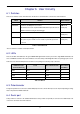
Chapter 2. Purpose This RSK is an evaluation tool for Renesas microcontrollers. This manual describes the technical details of the RSK hardware. The Quick Start Guide and Tutorial Manual provide details of the software installation and debugging environment. Features include: • Renesas Microcontroller Programming. • User Code Debugging. • User Circuitry such as Switches, LEDs and potentiometer. • User or Example Application. • Sample peripheral device initialisation code.
Chapter 3. Power Supply 3.1. Requirements This RSK operates from a 5V power supply. A diode provides reverse polarity protection only if a current limiting power supply is used. All RSK boards are supplied with an E10A debugger. All RSK boards have an optional centre positive supply connector using a 2.0mm barrel power jack. Warning The RSK is neither under nor over voltage protected. Use a centre positive supply for this board. 3.2.
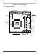
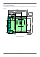
Chapter 4. Board Layout 4.1. Component Layout The following diagram shows top layer component layout of the board.
4.2. Board Dimensions The following diagram gives the board dimensions and connector positions. All through hole connectors are on a common 0.1” grid for easy interfacing.
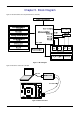
Chapter 5. Block Diagram Figure 5-1 shows the CPU board components and their connectivity. Figure 5-1: Block Diagram Figure 5-2 shows the connections to the RSK.
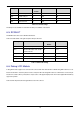
Chapter 6. User Circuitry 6.1. Switches There are four switches located on the CPU board. The function of each switch and its connection are shown in Table 6-1. Switch Function Microcontroller RES When pressed, the RSK microcontroller is reset. RESn, Pin 70(*) SW1/BOOT* Connects to an IRQ input for user controls. IRQ0, Pin 46 The switch is also used in conjunction with the RES switch to place the device in (Port B pin 2) BOOT mode when not using the E10A debugger.
Description Function Microcontroller Fit for RS232 Remove for RS232 Port Pin SCI2 Default serial port 58 R30 R53 SCI2 Default serial port 60 R39 R54 SCI0 Spare Serial Port 68 R53 R30 SCI0 Spare Serial Port 69 R54 R39 Table 6-3: Serial Port settings The SCI2 port is also available on J3 and JA6. The SCI0 port is available on J3 and JA2. 6.5. RCAN-ET The RCAN module can be used for RCAN communication. Table 6-4 contains details of the signal descriptions and pin connections.
LCD Pin Circuit Net Name Device Pin Circuit Net Name Device Pin Pin 1 Ground - 2 5V Only - 3 No Connection - 4 DLCDRS (PD10) 28 5 R/W (Wired to Write only) - 6 DLCDE + 100k pull down to ground (PD9) 29 7 No Connection - 8 No connection - 9 No Connection - 10 No connection - 11 DLCDD4 (PE0) 27 12 DLCDD5 (PE1) 26 13 DLCDD6 (PE2) 25 14 DLCDD7 (PE3) 24 Table 6-5 Debug LCD Module Connections 11
6.7. Option Links Table 6-6 below describes the function of the option links contained on this RSK board and associated with Serial Port Configuration. The default configuration is indicated by BOLD text. Option Link Settings Reference R54 Function Fitted Alternative (Removed) Serial Port Connects serial port SCI0 (Tx) to Disconnects serial port SCI0 Configuration D-type connector (SERIAL). (Tx) from D-type connector Related To R53 (SERIAL).
Option Link Settings Reference R159 R151 R148 R147 R146 R136 R137 R133 R128 R132 R129 R125 R102 R106 R107 R103 R99 R97 Function Fitted Alternative (Removed) Application Use TRSTn of E10A debugger Use M2_Wn of application board board interface interface. interface. Application Use M2_Wn of application board Use TRSTn of E10A debugger board interface interface. interface. Application Use TMS of E10A debugger Use M2_Vn of application board board interface interface interface.
Option Link Settings Reference R100 R98 R59 Function Fitted Alternative (Removed) Application Use TMR0 of application board Use A11 of application board board interface interface. interface. Application Use A11 of application board Use TMR0 of application board board interface interface. interface. Application Use to connect to onboard LED3.
Option Link Settings Reference R67 Function Fitted Alternative (Removed) Application Use A17 of application board Use SDA of application board board interface interface. interface “or” IRQ1 for onboard Related To R66, R68 SW2. R81 Application Use SCL of application board Use IRQ0 for onboard SW1 “or” board interface interface. A16 of application board R82, R83 interface. R83 Application Use IRQ0 for onboard SW1.
Option Link Settings Reference R93 R95 R112 R105 Function Fitted Alternative (Removed) Related To Application Use TXD2 for onboard RS232 Use IO1 of application board board interface module. interface. Application Use IO1 of application board Use TXD2 for onboard RS232 board interface interface. module. Application Use RXD2 for onboard RS232 Use WRLn, WRn “or” IO0 of R101, R105, board interface module. application board interface.
Option Link Settings Reference R118 R124 R121 Function Fitted Alternative (Removed) Application Use A1 of application board Use TXD0 for onboard RS232 board interface interface. module. Application Use RXD0 for onboard RS232 Use A0 of application board board interface module. interface. Application Use A0 of application board Use RXD0 for onboard RS232 board interface interface. module. Related To R120 R121 R124 Table 6-7: Application board interface links.
Option Link Settings Reference R33 Function MCU power Fitted Alternative (Removed) Supply to MCU. CPU current can be measured supply R161 R23 R24 R10 R3 Ground Power source Power source Power source Power source Related To across R33 Connects Analog & Digital Separates Analog & Digital grounds together. grounds. 5V source signal will be powered 5V source signal will not be from E8A_VCC. powered from E8A_VCC.
Option Link Settings Reference R49 Function Fitted Alternative (Removed) Voltage Voltage Reference set to board Voltage Reference taken from Reference Vcc signal. external connector (JA1 pin 7). Voltage Voltage Reference is taken from Voltage Reference set to board Reference external connector (JA1 pin 7). Vcc signal. Related To R50 Source R50 R49 Source Table 6-11: Voltage reference links. Table 6-12 below describes the function of the option links associated with analog power supply.
Option Link Settings Reference R46 Function Fitted Switches Alternative (Removed) SW3 can be used for ADTRGn R48 ADTRGn configuration R48 SW3 can not be used for Related To SW3 can be used for IRQ2 Switches SW3 can not be used for IRQ2 R46 configuration Table 6-14: Switches configuration links. 6.8. Oscillator Sources A crystal oscillator is fitted on the RSK and used to supply the main clock input to the Renesas microcontroller.
Chapter 7. Modes This RSK supports Boot mode, User Boot mode, User Program Mode and User mode. Details of programming the FLASH memory is described in the SH2/7137 Group Hardware Manual. 7.1. Boot mode The boot mode settings for this RSK are shown in Table 7-1: Boot Mode pin settings below: FWE MD2n MD1 1 0 0 LSI State after Reset End Boot Mode Table 7-1: Boot Mode pin settings The software supplied with this RSK supports debugging with E10A which does not need Boot mode.
7.5. MCU extension mode 0 CS0 space becomes external memory spaces with 8-bit bus width in SH7137. The MCU Extension Mode 0 settings for this RSK are shown in Table 7-5: MCU Extension Mode 0 pin settings below: FWE MD2n MD1 0 0 0 LSI State after Reset End MCU Extension Mode 0 Table 7-5: MCU Extension Mode 0 pin settings 7.6. MCU extension mode 2 CS0 space becomes external memory spaces with 8-bit bus width in SH7137.
Chapter 8. Programming Methods The board is intended for use with HEW and the supplied E10A debugger. Refer to SH2/7137 Group Hardware Manual for details of programming the microcontroller without using these tools.
Chapter 9. Headers 9.1. Microcontroller Headers Table 9-1 to Table 9-4 show the microcontroller pin headers and their corresponding microcontroller connections. The header pins connect directly to the microcontroller pin unless otherwise stated.
J2 Pin Circuit Net Name Device Pin Circuit Net Name Device Pin Pin 1 D7 31 2 D6 32 3 D5 33 4 D4 34 5 D3_LED3 35 6 UC_VCC - 7 D2_LED2 37 8 D1_LED1 38 9 GROUND 39 10 D0_LED0 40 11 CS1n_CRx0 41 12 CTx0 42 13 A19_CAN_STBn 43 14 A18_IRQ2 44 15 A17_IRQ1_SDA 45 16 A16_IRQ0_SCL 46 17 M2_TRISTn 47 18 UC_VCC - 19 UD_CAN_EN 49 20 GROUND - Table 9-2: J2 J3 Pin Circuit Net Name Device Pin Circuit Net Name Device Pin Pin 1 IO7 51 2 A10_IO6 5
J4 Pin Circuit Net Name Device Pin Circuit Net Name Pin Device Pin 1 AN14 81 2 AN13 82 3 AN12 83 4 PIN84 84 5 PIN85 85 6 PIN86 86 7 ADPOT 87 8 CON_AVREF 88 9 AN7 89 10 AN6 90 11 AN5 91 12 AN4 92 13 CON_AVSS 93 14 AN3 94 15 AN2 95 16 AN1 96 17 AN0 97 18 CON_AVCC 98 19 UC_VCC 99 20 WDT_OVFn 100 Table 9-4: J4 26
9.2. Application Headers Table 9-5 to Table 9-9 below show the standard application header connections.
JA2 Pin Generic Header Name CPU board Device Signal Name Pin Pin Generic Header Name CPU board Device Signal Name Pin 1 RESn RESn 70 2 EXTAL CON_EXTAL 72 3 NMIn NMI 73 4 VSS1 GROUND - 5 WDT_OVF WDT_OVFn 100 6 SCIaTX TxD0 68 7 IRQ0 IRQ0 46 8 SCIaRX RxD0 69 9 IRQ1 IRQ1 45 10 SCIaCK SCK0 67 11 UD UD 49 12 CTSRTS NC - 13 Up M1_Up 17 14 Un M1_Un 15 15 Vp M1_Vp 13 16 Vn M1_Vn 10 17 Wp M1_Wp 12 18 Wn M1_Wn 9 19 TMR0 TMR0 23 20
JA6 Pin Generic Header Name CPU board Device Signal Name Pin Pin Generic Header Name CPU board Device Signal Name Pin 1 DREQ NC - 2 DACK NC - 3 TEND NC - 4 STBYn NC - 5 RS232TX RS232TX - 6 RS232RX RS232RX - 7 SCIbRX NC - 8 SCIbTX NC - 9 SCIcTX TXD2 58 10 SCIbCK NC - 11 SCIcCK SCK2 61 12 SCIcRX RXD2 60 13 - - - 14 - - - 15 - - - 16 - - - 17 - - - 18 - - - 19 - - - 20 - - - 21 - - - 22 - - - 23 - - - 24 -
JA3 Pin Generic Header Name CPU board Device Signal Name Pin Pin Generic Header Name CPU board Device Signal Name Pin 1 A0 A0 69 2 A1 A1 68 3 A2 A2 67 4 A3 A3 66 5 A4 A4 65 6 A5 A5 63 7 A6 A6 56 8 A7 A7 55 9 A8 A8 54 10 A9 A9 53 11 A10 A10 52 12 A11 A11 23 13 A12 A12 22 14 A13 A13 21 15 A14 A14 20 16 A15 A15 19 17 D0 D0 40 18 D1 D1 38 19 D2 D2 37 20 D3 D3 35 21 D4 D4 34 22 D5 D5 33 23 D6 D6 32 24 D7 D7
Chapter 10. Code Development 10.1. Overview Note: For all code debugging using Renesas software tools, the RSK board must be connected to a PC USB port via an E10A. An E10A pod is supplied with the RSK product. 10.2. Compiler Restrictions The compiler supplied with this RSK is fully functional for a period of 60 days from first use. After the first 60 days of use have expired, the compiler will default to a maximum of 256K code and data.
10.5.
Chapter 11.
Chapter 12. Additional Information For details on how to use High-performance Embedded Workshop (HEW, refer to the HEW manual available on the CD or from the web site. For information about the SH2/7137 series microcontrollers refer to the SH7137 Group hardware manual. For information about the SH2/7137 assembly language, refer to the SH2 Series Software Manual. Online technical support and information is available at: http://www.renesas.
Renesas Starter Kit for SH2/7137 User's Manual Publication Date Rev.1.00 14.02.2008 Published by: Renesas Technology Europe Ltd. Duke’s Meadow, Millboard Road, Bourne End Buckinghamshire SL8 5FH, United Kingdom ©2008 Renesas Technology Europe and Renesas Solutions Corp., All Rights Reserved.
Renesas Starter Kit for SH2/7137 User's Manual Renesas Technology Europe Ltd.