
Datasheet

RJH1CV6DPK Preliminary
R07DS0747EJ0300 Rev.3.00 Page 2 of 9
Feb 14, 2013
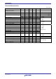
Electrical Characteristics
(Ta = 25°C)
Item Symbol Min Typ Max Unit Test Conditions
Zero gate voltage collector current
/ Diode reverse current
I
CES
/I
R
— — 5 A V
CE
= 1200 V, V
GE
= 0
Gate to emitter leak current I
GES
— — ±1 A V
GE
= ±30 V, V
CE
= 0
Gate to emitter cutoff voltage V
GE(off)
4.5 — 6.5 V V
CE
= 10 V, I
C
= 1 mA
V
CE(sat)
— 1.8 2.6 V I
C
= 30 A, V
GE
= 15 V
Note3
Collector to emitter saturation voltage
V
CE(sat)
— 2.6 — V I
C
= 60 A, V
GE
= 15 V
Note3
Input capacitance Cies — 1600 — pF
Output capacitance Coes — 85 — pF
Reverse transfer capacitance Cres — 43 — pF
V
CE
= 25 V
V
GE
= 0
f = 1 MHz
Total gate charge Qg — 105 — nC
Gate to emitter charge Qge — 14 — nC
Gate to collector charge Qgc — 55 — nC
V
GE
= 15 V
V
CE
= 300 V
I
C
= 35 A
Turn-on delay time t
d(on)
— 46 — ns
Rise time t
r
— 33 — ns
Turn-off delay time t
d(off)
— 125 — ns
Fall time t
f
— 120 — ns
Turn-on energy E
on
— 2.3 — mJ
Turn-off energy E
off
— 1.7 — mJ
Total switching energy E
total
— 4.0 — mJ
V
CC
= 600 V
V
GE
= 15 V
I
C
= 30 A
Rg = 5
Inductive load
Short circuit withstand time t
sc
— 5 — s
V
CC
720 V, V
GE
= 15 V
Tc 125°C
FRD forward voltage V
F
— 2.0 — V I
F
= 30 A
Note3
FRD reverse recovery time t
rr
— 180 — ns
FRD reverse recovery charge Q
rr
— 0.63 — C
FRD peak reverse recovery current I
rr
— 9.2 — A
I
F
= 30 A
di
F
/dt = 100 A/s
Notes: 3. Pulse test.