REG10J0049-0200 Renesas Starter Kit for R8C/2D User’s Manual RENESAS SINGLE-CHIP MICROCOMPUTER M16C FAMILY / R8C/Tiny SERIES Rev.2.00 Revision date: 12.OCT.2007 Renesas Solutions Corp. www.renesas.
Table of Contents Chapter 1. Preface ..................................................................................................................................................1 Chapter 2. Purpose .................................................................................................................................................2 Chapter 3. Power Supply ........................................................................................................................................
Chapter 1. Preface Cautions This document may be, wholly or partially, subject to change without notice. All rights reserved. Duplication of this document, either in whole or part is prohibited without the written permission of Renesas Solutions Corporation. Trademarks All brand or product names used in this manual are trademarks or registered trademarks of their respective companies or organisations. Copyright © Renesas Solutions Corp. 2007. All rights reserved. © Renesas Technology Europe Ltd. 2007.
Chapter 2. Purpose This Renesas Starter Kit is an evaluation tool for Renesas microcontrollers. Features include: • Renesas Microcontroller Programming. • User Code Debugging. • User Circuitry such as Switches, LEDs and potentiometer(s). • User or Example Application. • Sample peripheral device initialisation code. The Renesas Starter Kit board contains all the circuitry required for microcontroller operation.
Chapter 3. Power Supply 3.1. Requirements This Renesas Starter Kit operates from a 3V to 5V power supply. A diode provides reverse polarity protection only if a current limiting power supply is used. All Renesas Starter Kit boards are supplied with an E8a debugger. This product is able to power the Renesas Starter Kit board with up to 300mA. When the Renesas Starter Kit is connected to another system then that system should supply power to the Renesas Starter Kit.
Chapter 4. Board Layout 4.1. Component Layout The following diagram shows the top layer component layout of the board.
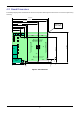
4.2. Board Dimensions The following diagram gives the board dimensions and connector positions. All through hole connectors are on a common 0.1” grid for easy interfacing. 120.00mm 115.00mm 86.36mm Short Board = 85 mm Corners x4 3mm radius 50.80 mm 43.18 mm 35.56 mm 27.00mm SW 1 SW 2 SW 3 RV1 (POT) JA2 L I N JA6 J4 - Applies to connector J3 E8 Serial D9 SKT JA5 JA1 R E S 14.00mm J2 3.81mm 5.00mm 45.00mm Figure 4-2 : Board Dimensions 5 100.00mm MC U 85.
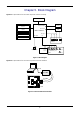
Chapter 5. Block Diagram Figure 5-1 is representative of the CPU board components and their connectivity.
Chapter 6. User Circuitry 6.1. Switches There are four switches located on the board. The function of each switch and its connection are shown in Table 6-1. Switch Function Microcontroller RES When pressed, the board microcontroller is reset. RESETn Pin9 SW1/BOOT* Connects to an IRQ input for user controls. INT0n Pin44 The switch is also used in conjunction with the RES switch to place (Port 4, pin 5) the device in BOOT mode when not using the E8A debugger.
6.4. Serial port This RSK provides two serial ports to the user. The serial port 1 has already been configured for use. To use serial port 2 the user needs to configure the option links as given in Table 6-3. Description Fit for RS232 TxD2 R34 RxD2 R33 Table 6-3: Serial Port settings 6.5. LCD Module A LCD module is supplied to be connected to the connector ‘LCD’. This should be fitted so that the LCD module lies over ‘JA1’ and ‘JA5’.
6.6. Option Links Table 6-5 below describes the function of the option links associated with Power configuration. The default configuration is indicated by BOLD text. Option Link Settings Reference R10 Function Power Source Fitted Board can be powered from Alternative (Removed) Related To Disable external power connector R44, R45 Supply power to Fit Low ohm resistor to measure - Microcontroller current. Connects external 5V supply Disconnects external 5V supply to the to the RSK. RSK.
Table 6-7 below describes the function of the option links associated with serial configuration. The default configuration is indicated by BOLD text. Option Link Settings Reference R11 R21 R22 R25 R30 R33 R34 R38 R39 Function Fitted Alternative (Removed) Related To Serial Port Connects serial port TXD1 to SERIAL Disconnects serial port TXD1 from Configuration D-type connector. SERIAL D-type connector.
Table 6-9 below describes the function of the option links associated with serial configuration. The default configuration is indicated by BOLD text.
The Reset circuit operates by latching the state of the boot switch on pressing the reset button. This control is subsequently used to modify the mode pin states as required. The MODE pin should change state only while the reset signal is active to avoid possible device damage. The reset is held in the active state for a fixed period by a pair of resistors and a capacitor.
Chapter 7. Modes This Renesas Starter Kit supports Boot mode and Single chip mode. Details of programming the FLASH memory is described in the R8C/2C Group, R8C/2D Group Hardware Manual. 7.1.
Chapter 8. Programming Methods The board is intended for use with High-performance Embedded Workshop and the supplied E8a debugger. Refer to R8C/2C Group, R8C/2D Group Hardware Manual for details of programming the microcontroller without using these tools.
Chapter 9. Headers 9.1. Microcontroller Headers Table 9-1 to Table 9-4 show the microcontroller pin headers and their corresponding microcontroller connections. The header pins connect directly to the microcontroller pins. * Marked pins are subject to option links.
J3 Pin Circuit Net Name Device Pin Pin Circuit Net Name Device Pin 1 DLCD5 41 2 DLCD4 42 3 LED0 43 4 INT0n 44 5 TXD1 45 6 RXD1_INT3n* 46 7 CLK2 47 8 RXD2 48 9 TXD2 49 10 TMR1 50 11 TMR0 51 12 INT1n 52 13 INT2n 53 14 AN11 54 15 AN10 55 16 AN9 56 17 ADPOT_AN8* 57 18 IO_7 58 19 IO_6 59 20 IO_5 60 Table 9-3: J3 J4 Pin Circuit Net Name Device Pin Pin Circuit Net Name Device Pin 1 IO_4 61 2 IO_3 62 3 IO_2 63 4 IO_1 64 5 IO_0 65
9.2. Application Headers Table 9-5 to Table 9-8 below show the standard application header connections. * Marked pins are subject to option links.
JA5 Pin Generic Header Name CPU board Device Signal Name Pin Pin Generic Header Name CPU board Device Signal Name Pin 1 AD4 AN4 69 2 AD5 AN5 68 3 AD6 AN6 67 4 AD7 AN7 66 5 CAN1TX --- --- 6 CAN1RX --- --- 7 CAN2TX --- --- 8 CAN2RX --- --- 9 AD8 AN8 57 10 AD9 AN9 56 11 AD10 AN10 55 12 AD11 AN11 54 13 TIOC0A TRCIOA 17 14 TIOC0B TRCIOB 16 15 TIOC0C TRCIOC 15 16 M2_TRISTn --- --- 17 TCLKC TRCCLK 18 18 TCLKD TRDCLK 30 19 M2_Up -
Table 9-9 below shows the LIN header connections.
Chapter 10. Code Development 10.1. Overview Note: For all code debugging using Renesas software tools, the Renesas Starter Kit board must be connected to a PC USB port via an E8a. An E8a is supplied with the Renesas Starter Kit product. 10.2. Mode Support High-performance Embedded Workspace connects to the Microcontroller and programs it via the E8a. Mode support is handled transparently to the user. 10.3.
10.4.
Chapter 11.
Chapter 12. Additional Information For details on how to use High-performance Embedded Workshop, refer to the High-performance Embedded Workshop manual available on the CD or from the web site. For information about the R8C/2D group microcontrollers, refer to the R8C/2C Group, R8C/2D Group Hardware Manual. For information about the R8C/2D assembly language, refer to the R8C/Tiny Series Software Programming Manual. Online technical support and information is available at: http://www.renesas.
Renesas Starter Kit for R8C/2D User's Manual Publication Date Rev.2.00 12.OCT.2007 Published by: Renesas Solutions Corp. Dukes Meadow, Millboard Road, Bourne End Buckinghamshire SL8 5FH, United Kingdom ©2007 Renesas Solutions Corp., Renesas Technology Europe Ltd. and Renesas Technology Corp., All Rights Reserved.
Renesas Starter Kit for R8C/2D User's Manual Renesas Solutions Corp.