REJ10J1242-0200 Renesas Starter Kit for R8C/25 User’s Manual RENESAS SINGLE-CHIP MICROCOMPUTER M16C FAMILY / R8C/Tiny SERIES Rev.2.00 Revision date: 15.OCT.2007 Renesas Solutions Corp. www.renesas.
Table of Contents Chapter 1. Preface ..................................................................................................................................................1 Chapter 2. Purpose .................................................................................................................................................2 Chapter 3. Power Supply ........................................................................................................................................
Chapter 1. Preface Cautions This document may be, wholly or partially, subject to change without notice. All rights reserved. Duplication of this document, either in whole or part is prohibited without the written permission of Renesas Solutions Corp. Trademarks All brand or product names used in this manual are trademarks or registered trademarks of their respective companies or organisations. Copyright © Renesas Solutions Corp. 2007. All rights reserved. © Renesas Technology Europe Ltd. 2007.
Chapter 2. Purpose This RSK is an evaluation tool for Renesas microcontrollers. Features include: • Renesas Microcontroller Programming. • User Code Debugging. • User Circuitry such as Switches, LEDs and potentiometer(s). • User or Example Application. • Sample peripheral device initialisation code. The RSK board contains all the circuitry required for microcontroller operation.
Chapter 3. Power Supply 3.1. Requirements This RSK operates from a 3V to 5V power supply. A diode provides reverse polarity protection only if a current limiting power supply is used. All RSK boards are supplied with an E8a debugger module. This product is able to power the RSK board with up to 300mA. When the RSK is connected to another system then that system should supply power to the RSK. All RSK boards have an optional centre positive supply connector using a 2.1mm barrel power jack.
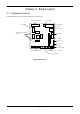
Chapter 4. Board Layout 4.1. Component Layout The following diagram shows the top layer component layout of the board.
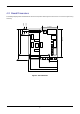
4.2. Board Dimensions The following diagram gives the board dimensions and connector positions. All through hole connectors are on a common 0.1” grid for easy interfacing. 3.81mm 5.00mm 45.00mm JA1 14.00mm 92.71mm 85.00mm 100.00mm MCU JA2 27.00mm 50.80mm 80.00mm 85.
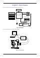
Chapter 5. Block Diagram Figure 5-1 is representative of the CPU board components and their connectivity.
Chapter 6. User Circuitry 6.1. Switches There are four switches located on the RSK. The function of each switch and its connection are shown in Table 6-1. Switch Function Microcontroller RES When pressed, the RSK microcontroller is reset. RESET Pin8 SW1/BOOT* Connects to an IRQ input for user controls. INT0 Pin27 The switch is also used in conjunction with the RES switch to place (Port 4, pin 5) the device in BOOT mode when not using the E8a debugger.
6.4. Serial port The microcontroller programming serial port 1 is connected to the RS232 transceiver. This serial port can optionally be connected to the RS232 transceiver as well by fitting option resistors. The connections to be fitted are listed in the table 6-3. Description Function Fit for RS232 TxD1 Programming Serial Port R45 RxD1 Programming Serial Port R46 Table 6-3: Serial Port settings A Secondary serial port is connected to the application headers. This is shared with the LIN module.
6.6.Option Links Table 6-5 below describes the function of the option links contained on this RSK board.
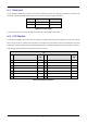
Option Link Settings Reference R22 R23 Function Board VCC Microcontroller Fitted Alternative (Removed) Connects External 3V3 External 3V3 disconnected (CON_3V3) to Board_VCC from Board_VCC Supply to microcontroller Fit Low ohm resister to Related To R20, R21 measure current VCC User I/O Power Connects Board_VCC supply Board_VCC disconnected from Supply to SW2, 3 and LED0-3 SW2, 3 and LED0-3 R31 SW1 Connects SW1 to INT0 Input Disconnected R44 RS232 Transceiver Disables RS232 Serial E
Option Link Settings Reference R64 R66 Function CAN CAN Fitted Alternative (Removed) Do not use CAN function, Do not use CAN function, R8C/25 Microcontroller do not R8C/25 Microcontroller do not have CAN function have CAN function Do not use CAN function, Do not use CAN function, R8C/25 Microcontroller do not R8C/25 Microcontroller do not have CAN function have CAN function Related To Table 6-5: Option Links 6.7.
Chapter 7. Modes The RSK supports Boot mode and Single chip mode. Details of programming the FLASH memory is described in the R8C/25 Group Hardware Manual. 7.1. Boot mode The boot mode settings for this RSK are shown in Table 7-1: Boot Mode pin settings below: MODE LSI State after Reset End Low Boot Mode Table 7-1: Boot Mode pin settings The software supplied with this RSK supports Boot mode using an E8a and HEW only.
Chapter 8. Programming Methods The board is intended for use with HEW and the supplied E8a debugger. Refer to R8C/25 Group Hardware Manual for details of programming the microcontroller without using these tools.
Chapter 9. Headers 9.1. Microcontroller Headers Table 9-1 to Table 9-4 show the microcontroller pin headers and their corresponding microcontroller connections. The header pins connect directly to the microcontroller pins. * Marked pins are subject to option links.
J3 Pin Circuit Net Name Device Pin Circuit Net Name Device Pin Pin 1 IRQ0/TRIGa* 27 2 IRQ1/IO_6* 28 3 IRQ2/IO_7* 29 4 LCD_E 30 5 LCD_RS 31 6 AD_POT 32 7 P3_1 33 8 TMR1 34 9 IO_5 35 10 IO_4 36 11 IO_3 37 12 AD0 38 13 No Connection - 14 No Connection - Table 9-3: J3 J4 Pin Circuit Net Name Device Pin Circuit Net Name Device Pin Pin 1 No Connection - 2 AD1 41 3 AD2 42 4 AD3 43 5 P4_2/VREF 44 6 IO_0 45 7 IO_2 46 8 IO_1 47 9 LCD_D7 4
9.2. Application Headers Table 9-5 and Table 9-6 below show the standard application header connections. * Marked pins are subject to option links.
J9 Pin Function Signal Name 1 Power Supply (for LIN module) VBAT 2 GROUND GND J10 Pin Function Signal Name 1 Power Supply (for LIN module) VBAT 2 LIN Bus Line LIN 3 GROUND GND Table 9-7: LIN Headers 17
Chapter 10.Code Development 10.1. Overview Note: For all code debugging using Renesas software tools, the RSK board must be connected to a PC USB port via an E8a. An E8a is supplied with the RSK product. 10.2. Mode Support HEW connects to the Microcontroller and programs it via the E8a. Mode support is handled transparently to the user. 10.3. Breakpoint Support HEW supports breakpoints on the user code, both in RAM and ROM. Double clicking in the breakpoint column in the code sets the breakpoint.
10.4.
Chapter 11.
Chapter 12. Additional Information For details on how to use High-performance Embedded Workshop (HEW, refer to the HEW manual available on the CD or from the web site. For information about the R8C/25 group microcontrollers refer to the R8C/25 Group Hardware Manual For information about the R8C/25 assembly language, refer to the R8C/Tiny Series Software Programming Manual. Online technical support and information is available at: http://www.renesas.com/rsk Technical Contact Details America: techsupport.
Renesas Starter Kit for R8C/25 User's Manual Publication Date Rev.1.01 29.05.2006 Published by: Renesas Solutions Corp. 4-1-6, Miyahara, Yodogawa-ku, Osaka City, 532-0003, Japan ©2006 Renesas Solutions Corp., Renesas Technology Europe Ltd. and Renesas Technology Corp., All Rights Reserved.
Renesas Starter Kit for R8C/25 User's Manual Renesas Solutions Corp.