
Datasheet

R01DS0031EJ0210 Rev.2.10 Page 82 of 111
Jul 31, 2012
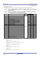
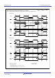
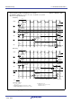
M16C/65 Group 5. Electrical Characteristics
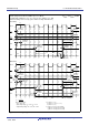
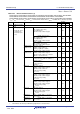
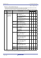
Figure 5.17 Timing Diagram
Memory Expansion Mode and Microprocessor Mode
(in 2 or 3 waits setting, and when accessing external area and using multiplexed bus)
BCLK
CSi
ADi
ALE
RD
BHE
ADi
/DBi
Read timing
BCLK
CSi
ADi
ALE
BHE
ADi
/DBi
Data output
Write timing
Address
Address
Data input
Address
Address
V = V = 5V
CC1 CC2
t
d(BCLK-CS)
25ns(max.)
t
cyc
(0.5 × t -10)ns(min.)
cyc
t
h(RD-CS)
t
h(BCLK-CS)
0ns(min.)
(0.5 × t -25ns(min.)
cyc
t
d(AD-ALE)
(0.5 × t -15ns(min.)
cyc
t
h(ALE-AD)
t
dz(RD-AD)
8ns(max.)
{(n-0.5) × t -45}ns(max.)
cyc
t
ac3(RD-DB)
t
su(DB-RD)
t
h(RD-DB)
0ns(min.)
0ns(min.)
t
d(AD-RD)
t
h(BCLK-AD)
0ns(min.)
15ns(max.)
t
d(BCLK-ALE)
t
h(BCLK-ALE)
-4ns(min.)
t
d(BCLK-AD)
25ns(max.)
t
h(RD-AD)
(0.5 × t -10)ns(min.)
cyc
25ns(max.)
t
d(BCLK-RD)
0ns(min.)
t
h(BCLK-RD)
t
cyc
t
d(BCLK-CS)
25ns(max.)
(0.5 × t -10)ns(min.)
cyc
t
h(WR-CS)
t
h(BCLK-CS)
0ns(min.)
t
d(BCLK-DB)
40ns(max.)
t
h(BCLK-DB)
0ns(min.)
(0.5 × t -25ns(min.)
cyc
t
d(AD-ALE)
{(n-0.5) × t -40}ns(min.)
cyc
t
d(DB-WR)
(0.5 × t -10)ns(min.)
cyc
t
h(WR-DB)
t
d(BCLK-AD)
25ns(max.)
t
h(BCLK-AD)
0ns(min.)
15ns(max.)
t
d(BCLK-ALE)
t
h(BCLK-ALE)
-4ns(min.) 0ns(min.)
t
d(AD-WR)
t
h(WR-AD)
(0.5 × t -10)ns(min.)
cyc
25ns(max.)
t
d(BCLK-WR)
0ns(min.)
t
h(BCLK-WR)
n: 2 (when 2 waits)
3 (when 3 waits)
Measuring conditions
y V
= V = 5V
CC1 CC2
y Input timing voltage: V = 0.8 V, V = 2.0 V
IL IH
y Output timing voltage: V = 0.4 V, V = 2.4 V
OL OH
40ns(min.)
WR, WRL,
WRH