
Datasheet


R8C/L35C Group, R8C/L36C Group, R8C/L38C Group, R8C/L3AC Group 5. Electrical Characteristics
R01DS0095EJ0101 Rev.1.01 Page 57 of 72
Apr 15, 2011
Notes:
1. Vcc = 4.0 V to 5.5 V, single chip mode, output pins are open, and other pins are Vss.
2. XIN is set to square wave input.
3. Vcc = 5.0 V
4. VLCD = Vcc, external division resistors are used for VL4 to VL1, 1/3 bias, 1/4 duty, f(FR) = 64 Hz, SEG0 to SEG55 are selected, and segment
and common output pins are open. The standard value does not include the current that flows through external division resistors.
5. The internal voltage multiplier is used, bits LVLS3 to LVLS0 in the LCR1 register = 1011b, 1/3 bias, 1/4 duty, f(FR) = 64 Hz, SEG0 to SEG55
are selected, and segment and common output pins are open.
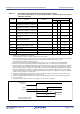
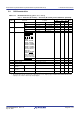
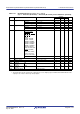
Table 5.18 DC Characteristics (2) [4.0 V ≤ Vcc ≤ 5.5 V]
(T
opr = −20 to 85°C (N version) / −40 to 85°C (D version), unless otherwise specified.)
Symbol Parameter
Condition Standard
Unit
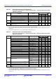
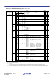
Oscillation
Circuit
On-Chip
Oscillator
CPU
Clock
Low-Power-
Consumption
Setting
Other Min.
Typ.
(3)
Max.
XIN
(2)
XCIN
High-Speed
(fOCO-F)
Low-
Speed
I
CC Power
supply
current
(1)
High-
speed
clock
mode
20
MHz
Off Off 125
kHz
No
division
——7.015mA
16
MHz
Off Off 125
kHz
No
division
— — 5.6 12.5 mA
10
MHz
Off Off 125
kHz
No
division
——3.6—mA
20
MHz
Off Off 125
kHz
Divide-
by-8
——3.0—mA
16
MHz
Off Off 125
kHz
Divide-
by-8
——2.2—mA
10
MHz
Off Off 125
kHz
Divide-
by-8
——1.5—mA
High-
speed
on-chip
oscillator
mode
Off Off 20 MHz 125
kHz
No
division
——7.015mA
Off Off 20 MHz 125
kHz
Divide-
by-8
——3.0—mA
Off Off 4 MHz 125
kHz
Divide-
by-16
MSTIIC = 1
MSTTRD = 1
MSTTRC = 1
MSTTRG = 1
—1—mA
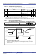
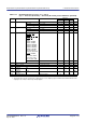
Low-
speed
on-chip
oscillator
mode
Off Off Off 125
kHz
Divide-
by-8
FMR27 = 1
VCA20 = 0
— 90 400
µA
Low-
speed
clock
mode
Off 32
kHz
Off Off No
division
FMR27 = 1
VCA20 = 0
— 100 400
µA
Off 32
kHz
Off Off No
division
FMSTP = 1
VCA20 = 0
Flash memory off
Program operation on RAM
—55—
µA
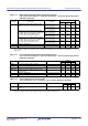
Wait
mode
Off Off Off 125
kHz
— VCA27 = 0
VCA26 = 0
VCA25 = 0
VCA20 = 1
While a WAIT instruction is executed
Peripheral clock operation
— 15 100
µA
Off Off Off 125
kHz
— VCA27 = 0
VCA26 = 0
VCA25 = 0
VCA20 = 1
CM02 = 1
CM01 = 1
While a WAIT instruction is executed
Peripheral clock off
—490
µA
Off 32
kHz
Off Off — VCA27 = 0
VCA26 = 0
VCA25 = 0
VCA20 = 1
CM02 = 1
CM01 = 0
While a WAIT
instruction is executed
Peripheral clock off
Timer RE operation in
real-time clock mode
LCD drive control
circuit
(4)
When external division
resistors are used
—7—µA
LCD drive control
circuit
(5)
When the internal
voltage multiplier is used
—12—µA
Off 32
kHz
Off Off — VCA27 = 0
VCA26 = 0
VCA25 = 0
VCA20 = 1
CM02 = 1
CM01 = 1
While a WAIT instruction is executed
Peripheral clock off
Timer RE operation in real-time clock mode
—3.5—
µA
Stop
mode
Off Off Off Off — VCA27 = 0
VCA26 = 0
VCA25 = 0
CM10 = 1
Topr = 25
°C
Peripheral clock off
—2.05.0µA
Off Off Off Off — VCA27 = 0
VCA26 = 0
VCA25 = 0
CM10 = 1
Topr = 85
°C
Peripheral clock off
—15—µA
Power-
off mode
Off Off Off Off — — Topr = 25°C — 0.02 0.2 µA
Off Off Off Off — — Topr = 85
°C—0.4—µA