
Datasheet


R8C/L35C Group, R8C/L36C Group, R8C/L38C Group, R8C/L3AC Group 5. Electrical Characteristics
R01DS0095EJ0101 Rev.1.01 Page 52 of 72
Apr 15, 2011
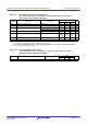
Notes:
1. Select the voltage detection level with bits VDSEL0 and VDSEL1 in the OFS register.
2. Necessary time until the voltage detection circuit operates when setting to 1 again after setting the VCA25 bit in the VCA2
register to 0.
3. Time until the voltage monitor 0 reset is generated after the voltage passes V
det0.
Notes:
1. Select the voltage detection level with bits VD1S0 to VD1S3 in the VD1LS register.
2. Time until the voltage monitor 1 interrupt request is generated after the voltage passes V
det1.
3. Necessary time until the voltage detection circuit operates when setting to 1 again after setting the VCA26 bit in the VCA2
register to 0.
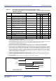
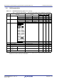
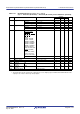
Table 5.8 Voltage Detection 0 Circuit Characteristics
(V
CC = 1.8 to 5.5 V and Topr = −20 to 85°C (N version) / −40 to 85°C (D version), unless
otherwise specified.)
Symbol Parameter Condition
Standard
Unit
Min. Typ. Max.
V
det0
Voltage detection level Vdet0_0
(1)
1.80 1.90 2.05 V
Voltage detection level Vdet0_1
(1)
2.15 2.35 2.50 V
Voltage detection level Vdet0_2
(1)
2.70 2.85 3.05 V
Voltage detection level Vdet0_3
(1)
3.55 3.80 4.05 V
—
Voltage detection 0 circuit response time
(3)
At the falling of Vcc from 5 V
to (Vdet0_0
− 0.1) V
— 6 150
µs
— Voltage detection circuit self power consumption VCA25 = 1, V
CC = 5.0 V — 1.5 — µA
t
d(E-A) Waiting time until voltage detection circuit
operation starts
(2)
— — 100 µs
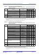
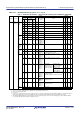
Table 5.9 Voltage Detection 1 Circuit Characteristics
(V
CC = 1.8 to 5.5 V and Topr = −20 to 85°C (N version) / −40 to 85°C (D version), unless
otherwise specified.)
Symbol Parameter Condition
Standard
Unit
Min. Typ. Max.
V
det1
Voltage detection level Vdet1_0
(1)
At the falling of VCC
2.00 2.20 2.40 V
Voltage detection level Vdet1_1
(1)
At the falling of VCC
2.15 2.35 2.55 V
Voltage detection level Vdet1_2
(1)
At the falling of VCC
2.30 2.50 2.70 V
Voltage detection level Vdet1_3
(1)
At the falling of VCC
2.45 2.65 2.85 V
Voltage detection level Vdet1_4
(1)
At the falling of VCC
2.60 2.80 3.00 V
Voltage detection level Vdet1_5
(1)
At the falling of VCC
2.75 2.95 3.15 V
Voltage detection level Vdet1_6
(1)
At the falling of VCC
2.85 3.10 3.40 V
Voltage detection level Vdet1_7
(1)
At the falling of VCC
3.00 3.25 3.55 V
Voltage detection level Vdet1_8
(1)
At the falling of VCC
3.15 3.40 3.70 V
Voltage detection level Vdet1_9
(1)
At the falling of VCC
3.30 3.55 3.85 V
Voltage detection level Vdet1_A
(1)
At the falling of VCC
3.45 3.70 4.00 V
Voltage detection level Vdet1_B
(1)
At the falling of VCC
3.60 3.85 4.15 V
Voltage detection level Vdet1_C
(1)
At the falling of VCC
3.75 4.00 4.30 V
Voltage detection level Vdet1_D
(1)
At the falling of VCC
3.90 4.15 4.45 V
Voltage detection level Vdet1_E
(1)
At the falling of VCC
4.05 4.30 4.60 V
Voltage detection level Vdet1_F
(1)
At the falling of VCC
4.20 4.45 4.75 V
— Hysteresis width at the rising of Vcc in voltage
detection 1 circuit
Vdet1_0 to Vdet1_5
selected
—0.07— V
Vdet1_6 to Vdet1_F
selected
—0.10— V
—
Voltage detection 1 circuit response time
(2)
At the falling of Vcc from
5 V to (Vdet1_0
− 0.1) V
— 60 150
µs
— Voltage detection circuit self power consumption VCA26 = 1, V
CC = 5.0 V — 1.7 — µA
t
d(E-A) Waiting time until voltage detection circuit operation
starts
(3)
— — 100 µs