
Datasheet


R8C/L35C Group, R8C/L36C Group, R8C/L38C Group, R8C/L3AC Group 5. Electrical Characteristics
R01DS0095EJ0101 Rev.1.01 Page 48 of 72
Apr 15, 2011
5.3 Peripheral Function Characteristics
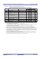
Notes:
1. The A/D conversion result will be undefined in wait mode, stop mode, power-off mode, when the flash memory stops, and in
low-current-consumption mode. Do not perform A/D conversion in these states or transition to these states during A/D
conversion.
2. This applies when the peripheral functions are stopped.
3. When the analog input voltage is over the reference voltage, the A/D conversion result will be 3FFh in 10-bit mode and FFh in
8-bit mode.
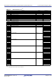
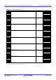
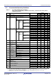
Table 5.3 A/D Converter Characteristics
(V
CC
/AV
CC
= Vref = 2.2 to 5.5 V, V
SS
= 0 V, and T
opr
=
−
20 to 85
°
C (N version) /
−
40 to 85
°
C (D version), unless otherwise specified.)
Symbol Parameter Conditions
Standard
Unit
Min. Typ. Max.
— Resolution V
ref = AVCC ——10Bit
—
Absolute accuracy
(2)
10-bit mode Vref = AVCC = 5.0 V AN0 to AN19 input — — ±3 LSB
V
ref = AVCC = 3.3 V AN0 to AN19 input — — ±5 LSB
V
ref = AVCC = 3.0 V AN0 to AN19 input — — ±5 LSB
V
ref = AVCC = 2.2 V AN0 to AN19 input — — ±5 LSB
8-bit mode V
ref = AVCC = 5.0 V AN0 to AN19 input — — ±2 LSB
V
ref = AVCC = 3.3 V AN0 to AN19 input — — ±2 LSB
V
ref = AVCC = 3.0 V AN0 to AN19 input — — ±2 LSB
V
ref = AVCC = 2.2 V AN0 to AN19 input — — ±2 LSB
φAD A/D conversion clock
4.0
≤ Vref = AVCC ≤ 5.5 V
(1)
2—20MHz
3.2
≤ Vref = AVCC ≤ 5.5 V
(1)
2—16MHz
2.7
≤ Vref = AVCC ≤ 5.5 V
(1)
2—10MHz
2.2
≤ Vref = AVCC ≤ 5.5 V
(1)
2—5MHz
— Tolerance level impedance — 3 — k
Ω
tCONV Conversion time 10-bit mode Vref = AVCC = 5.0 V, φAD = 20 MHz 2.2 — — µs
8-bit mode V
ref = AVCC = 5.0 V, φAD = 20 MHz 2.2 — — µs
t
SAMP Sampling time φAD = 20 MHz 0.8 — — µs
I
Vref Vref current Vcc = 5 V, XIN = f1 = φAD = 20 MHz — 45 — µA
V
ref Reference voltage 2.2 — AVCC V
V
IA
Analog input voltage
(3)
0—Vref V
OCVREF On-chip reference voltage 2 MHz
≤ φAD ≤ 4 MHz 1.19 1.34 1.49 V