
Datasheet


R8C/32D Group 1. Overview
REJ03B0288-0100 Rev.1.00 Feb 26, 2010
Page 6 of 42
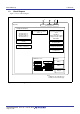
1.4 Pin Assignment
Figure 1.3 shows Pin Assignment (Top View). Table 1.4 outlines the Pin Name Information by Pin Number.
Figure 1.3 Pin Assignment (Top View)
1
2
3
4
5
6
7
8
9
10
20 P1_0/AN8/KI0(/TRCIOD)
19 P1_1/AN9/KI1(/TRCIOA/TRCTRG)
18 P1_2/AN10/Kl2(/TRCIOB)
17 P1_3/AN11/Kl3/TRBO(/TRCIOC)
16 P1_4(/TXD0/TRCCLK)
15 P1_5(/INT1/RXD0/TRAIO)
14 P1_6/IVREF1(/CLK0)
13 P1_7/IVCMP1/INT1(/TRAIO)
12 P4_5/ADTRG/INT0(/RXD2/SCL2)
11 P3_3/IVCMP3/INT3(/CTS2/RTS2/TRCCLK)
P4_2/VREF
MODE
RESET
P4_7/XOUT(/XCOUT)
VSS/AVSS
P4_6/XIN(/XCIN)
VCC/AVCC
P3_7/TRAO(/RXD2/SCL2/TXD2/SDA2)
P3_5(/CLK2/TRCIOD)
P3_4/IVREF3(/RXD2/SCL2/TXD2/SDA2/TRCIOC)
R8C/32D Group
PLSP0020JB-A
(20P2F-A)
(top view)
Notes:
1. Can be assigned to the pin in parentheses by a program.
2. Confirm the pin 1 position on the package by referring to the package dimensions.