
Datasheet


R8C/32D Group 5. Electrical Characteristics
REJ03B0288-0100 Rev.1.00 Feb 26, 2010
Page 41 of 42
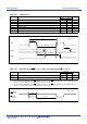
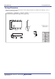
i = 0, 2
Figure 5.14 Serial Interface Timing Diagram when VCC = 2.2 V
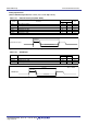
Notes:
1. When selecting the digital filter by the INTi
input filter select bit, use an INTi input HIGH width of either (1/digital filter clock
frequency × 3) or the minimum value of standard, whichever is greater.
2. When selecting the digital filter by the INTi
input filter select bit, use an INTi input LOW width of either (1/digital filter clock
frequency × 3) or the minimum value of standard, whichever is greater.
Figure 5.15 Input Timing for External Interrupt INT
i and Key Input Interrupt KIi when Vcc = 2.2 V
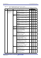
Table 5.29 Serial Interface
Symbol Parameter
Standard
Unit
Min. Max.
t
c(CK) CLKi input cycle time 800 − ns
tW(CKH) CLKi input “H” width 400 − ns
tW(CKL) CLKi input “L” width 400 − ns
td(C-Q) TXDi output delay time − 200 ns
th(C-Q) TXDi hold time 0 − ns
tsu(D-C) RXDi input setup time 150 − ns
th(C-D) RXDi input hold time 90 − ns
Table 5.30 External Interrupt INTi
(i = 0, 1, 3) Input, Key Input Interrupt KIi (i = 0 to 3)
Symbol Parameter
Standard
Unit
Min. Max.
tW(INH)
INTi
input “H” width, KIi input “H” width
1000
(1)
− ns
tW(INL)
INTi
input “L” width, KIi input “L” width
1000
(2)
− ns
tW(CKH)
tC(CK)
tW(CKL)
th(C-Q)
th(C-D)
tsu(D-C)td(C-Q)
CLKi
TXDi
RXDi
VCC = 2.2 V
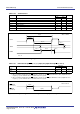
i = 0, 2
tW(INL)
tW(INH)
VCC = 2.2 V
INTi input
(i = 0, 1, 3)
KIi input
(i = 0 to 3)