
Datasheet


R8C/32D Group 5. Electrical Characteristics
REJ03B0288-0100 Rev.1.00 Feb 26, 2010
Page 28 of 42
Notes:
1. The measurement condition is VCC = 1.8 V to 5.5 V and Topr = −20 to 85°C (N version) / −40 to 85°C (D version).
2. Time until the voltage monitor 2 interrupt request is generated after the voltage passes Vdet2.
3. Necessary time until the voltage detection circuit operates after setting to 1 again after setting the VCA27 bit in the VCA2
register to 0.
Notes:
1. The measurement condition is T
opr = −20 to 85°C (N version) / −40 to 85°C (D version), unless otherwise specified.
2. To use the power-on reset function, enable voltage monitor 0 reset by setting the LVDAS bit in the OFS register to 0.
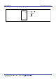
Figure 5.3 Power-on Reset Circuit Electrical Characteristics
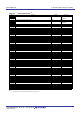
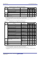
Table 5.8 Voltage Detection 2 Circuit Electrical Characteristics
Symbol Parameter Condition
Standard
Unit
Min. Typ. Max.
V
det2 Voltage detection level Vdet2_0 At the falling of VCC 3.70 4.00 4.30 V
− Hysteresis width at the rising of Vcc in voltage detection
2 circuit
− 0.10 − V
−
Voltage detection 2 circuit response time
(2)
At the falling of Vcc from
5 V to (Vdet2_0 − 0.1) V
− 20 150 µs
− Voltage detection circuit self power consumption VCA27 = 1, VCC = 5.0 V − 1.7 −µA
td(E-A) Waiting time until voltage detection circuit operation
starts
(3)
−−100 µs
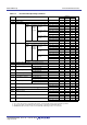
Table 5.9 Power-on Reset Circuit
(2)
Symbol Parameter Condition
Standard
Unit
Min. Typ. Max.
t
rth External power VCC rise gradient
(1)
0 − 50000 mV/msec
Notes:
1. Vdet0 indicates the voltage detection level of the voltage detection 0 circuit. Refer to 6. Voltage Detection
Circuit of Hardware Manual (REJ09B0528) for details.
2. tw(por) indicates the duration the external power VCC must be held below the valid voltage (0.5 V) to enable
a power-on reset. When turning on the power after it falls with voltage monitor 0 reset disabled, maintain
t
w(por) for 1 ms or more.
Vdet0
(1)
0.5 V
Internal
reset signal
tw(por)
(2)
Voltage detection 0
circuit response time
Vdet0
(1)
1
fOCO-S
× 32
1
fOCO-S
× 32
External
Power VCC
trth
trth