
Datasheet


R8C/32D Group 5. Electrical Characteristics
REJ03B0288-0100 Rev.1.00 Feb 26, 2010
Page 25 of 42
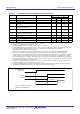
Notes:
1. VCC/AVCC = Vref = 2.2 to 5.5 V, VSS = 0 V at Topr = −20 to 85°C (N version) / −40 to 85°C (D version), unless otherwise
specified.
2. The A/D conversion result will be undefined in wait mode, stop mode, when the flash memory stops, and in low-current-
consumption mode. Do not perform A/D conversion in these states or transition to these states during A/D conversion.
3. When the analog input voltage is over the reference voltage, the A/D conversion result will be 3FFh in 10-bit mode and FFh in
8-bit mode.
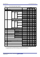
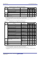
Notes:
1. V
CC = 2.7 to 5.5 V, Topr = −20 to 85°C (N version) / −40 to 85°C (D version), unless otherwise specified.
2. When the digital filter is disabled.
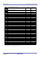
Table 5.3 A/D Converter Characteristics
Symbol Parameter Conditions
Standard
Unit
Min. Typ. Max.
− Resolution V
ref = AVCC −−10 Bit
− Absolute accuracy 10-bit mode Vref = AVCC = 5.0 V AN8 to AN11 input −−±3 LSB
Vref = AVCC = 3.3 V AN8 to AN11 input −−±5 LSB
Vref = AVCC = 3.0 V AN8 to AN11 input −−±5 LSB
Vref = AVCC = 2.2 V AN8 to AN11 input −−±5 LSB
8-bit mode Vref = AVCC = 5.0 V AN8 to AN11 input −−±2 LSB
Vref = AVCC = 3.3 V AN8 to AN11 input −−±2 LSB
Vref = AVCC = 3.0 V AN8 to AN11 input −−±2 LSB
Vref = AVCC = 2.2 V AN8 to AN11 input −−±2 LSB
φAD A/D conversion clock
4.0 V ≤ Vref = AVCC ≤ 5.5 V
(2)
2 − 20 MHz
3.2 V ≤ Vref = AVCC ≤ 5.5 V
(2)
2 − 16 MHz
2.7 V ≤ Vref = AVCC ≤ 5.5 V
(2)
2 − 10 MHz
2.2 V ≤ Vref = AVCC ≤ 5.5 V
(2)
2 − 5MHz
− Tolerance level impedance − 3 − kΩ
tCONV Conversion time 10-bit mode Vref = AVCC = 5.0 V, φAD = 20 MHz 2.15 −−µs
8-bit mode Vref = AVCC = 5.0 V, φAD = 20 MHz 2.15 −−µs
tSAMP Sampling time φAD = 20 MHz 0.75 −−µs
IVref Vref current VCC = 5 V, XIN = f1 = φAD = 20 MHz − 45 −µA
Vref Reference voltage 2.2 − AVCC V
VIA
Analog input voltage
(3)
0 − Vref V
OCVREF On-chip reference voltage 2 MHz ≤ φAD ≤ 4 MHz 1.19 1.34 1.49 V
Table 5.4 Comparator B Electrical Characteristics
Symbol Parameter Condition
Standard
Unit
Min. Typ. Max.
Vref IVREF1, IVREF3 input reference voltage 0 − VCC − 1.4 V
VI IVCMP1, IVCMP3 input voltage −0.3 − VCC + 0.3 V
− Offset − 5 100 mV
td
Comparator output delay time
(2)
VI = Vref ± 100 mV − 0.1 −µs
ICMP Comparator operating current VCC = 5.0 V − 17.5 −µA