
Datasheet


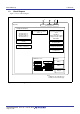


R8C/32D Group 1. Overview
REJ03B0288-0100 Rev.1.00 Feb 26, 2010
Page 8 of 42
1.5 Pin Functions
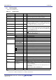
Table 1.5 lists Pin Functions.
I: Input O: Output I/O: Input and output
Note:
1. Refer to the oscillator manufacturer for oscillation characteristics.
Table 1.5 Pin Functions
Item Pin Name
I/O Type
Description
Power supply input VCC, VSS − Apply 1.8 V to 5.5 V to the VCC pin. Apply 0 V to the VSS pin.
Analog power
supply input
AVCC, AVSS − Power supply for the A/D converter.
Connect a capacitor between AVCC and AVSS.
Reset input RESET
I Input “L” on this pin resets the MCU.
MODE MODE I Connect this pin to VCC via a resistor.
XIN clock input XIN I These pins are provided for XIN clock generation circuit I/O.
Connect a ceramic resonator or a crystal oscillator between
the XIN and XOUT pins
(1)
. To use an external clock, input it
to the XOUT pin and leave the XIN pin open.
XIN clock output XOUT I/O
XCIN clock input XCIN I These pins are provided for XCIN clock generation circuit I/O.
Connect a crystal oscillator between the XCIN and XCOUT
pins
(1)
. To use an external clock, input it to the XCIN pin and
leave the XCOUT pin open.
XCIN clock output XCOUT O
INT
interrupt input INT0, INT1, INT3 IINT interrupt input pins.
INT0
is timer RB, and RC input pin.
Key input interrupt
KI0
to KI3
I Key input interrupt input pins
Timer RA TRAIO I/O Timer RA I/O pin
TRAO O Timer RA output pin
Timer RB TRBO O Timer RB output pin
Timer RC TRCCLK I External clock input pin
TRCTRG I External trigger input pin
TRCIOA, TRCIOB,
TRCIOC, TRCIOD
I/O Timer RC I/O pins
Serial interface CLK0, CLK2 I/O Transfer clock I/O pins
RXD0, RXD2 I Serial data input pins
TXD0, TXD2 O Serial data output pins
CTS2
I Transmission control input pin
RTS2
O Reception control output pin
SCL2 I/O
I
2
C mode clock I/O pin
SDA2 I/O
I
2
C mode data I/O pin
Reference voltage
input
VREF I Reference voltage input pin to A/D converter
A/D converter AN8 to AN11 I Analog input pins to A/D converter
ADTRG
I A/D external trigger input pin
Comparator B IVCMP1, IVCMP3 I Comparator B analog voltage input pins
IVREF1, IVREF3 I Comparator B reference voltage input pins
I/O port P1_0 to P1_7,
P3_3 to P3_5, P3_7,
P4_5 to P4_7
I/O CMOS I/O ports. Each port has an I/O select direction
register, allowing each pin in the port to be directed for input
or output individually.
Any port set to input can be set to use a pull-up resistor or not
by a program.
All ports can be used as LED drive ports.
Input port P4_2 I Input-only port