To our customers, Old Company Name in Catalogs and Other Documents On April 1st, 2010, NEC Electronics Corporation merged with Renesas Technology Corporation, and Renesas Electronics Corporation took over all the business of both companies. Therefore, although the old company name remains in this document, it is a valid Renesas Electronics document. We appreciate your understanding. Renesas Electronics website: http://www.renesas.
Notice 1. 2. 3. 4. 5. 6. 7. All information included in this document is current as of the date this document is issued. Such information, however, is subject to change without any prior notice. Before purchasing or using any Renesas Electronics products listed herein, please confirm the latest product information with a Renesas Electronics sales office.
R8C/32D Group REJ03B0288-0100 Rev.1.00 Feb 26, 2010 RENESAS MCU 1. Overview 1.1 Features The R8C/32D Group of single-chip MCUs incorporates the R8C CPU core, employing sophisticated instructions for a high level of efficiency. With 1 Mbyte of address space, and it is capable of executing instructions at high speed. In addition, the CPU core boasts a multiplier for high-speed operation processing. Power consumption is low, and the supported operating modes allow additional power control.
R8C/32D Group 1.1.2 1. Overview Specifications Tables 1.1 and 1.2 outline the Specifications for R8C/32D Group. Table 1.1 Item CPU Specifications for R8C/32D Group (1) Function Central processing unit Memory Power Supply Voltage Detection I/O Ports ROM, RAM Voltage detection circuit Clock Clock generation circuits Programmable I/O ports Interrupts Watchdog Timer Timer Timer RA Timer RB Timer RC Timer RE Serial Interface UART0 UART2 A/D Converter Comparator B REJ03B0288-0100 Rev.1.
R8C/32D Group Table 1.2 Item Flash Memory 1. Overview Specifications for R8C/32D Group (2) Function Operating Frequency/Supply Voltage Current consumption Operating Ambient Temperature Package Specification • Programming and erasure voltage: VCC = 2.7 to 5.5 V • Programming and erasure endurance: 1,000 times (program ROM) • Program security: ROM code protect, ID code check • Debug functions: On-chip debug, on-board flash rewrite function f(XIN) = 20 MHz (VCC = 2.7 to 5.5 V) f(XIN) = 5 MHz (VCC = 1.
R8C/32D Group 1.2 1. Overview Product List Table 1.3 lists Product List for R8C/32D Group, and Figure 1.1 shows a Part Number, Memory Size, and Package of R8C/32D Group. Table 1.3 Product List for R8C/32D Group Part No. R5F21321DNSP R5F21322DNSP R5F21324DNSP R5F21321DDSP (D) R5F21322DDSP (D) R5F21324DDSP (D) ROM Capacity 4 Kbytes 8 Kbytes 16 Kbytes 4 Kbytes 8 Kbytes 16 Kbytes Current of Feb.
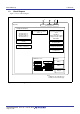
R8C/32D Group 1.3 1. Overview Block Diagram Figure 1.2 shows a Block Diagram.
R8C/32D Group 1.4 1. Overview Pin Assignment Figure 1.3 shows Pin Assignment (Top View). Table 1.4 outlines the Pin Name Information by Pin Number.
R8C/32D Group Table 1.4 1.
R8C/32D Group 1.5 1. Overview Pin Functions Table 1.5 lists Pin Functions. Table 1.5 Pin Functions Item Pin Name I/O Type Description Power supply input VCC, VSS − Apply 1.8 V to 5.5 V to the VCC pin. Apply 0 V to the VSS pin. Analog power supply input AVCC, AVSS − Power supply for the A/D converter. Connect a capacitor between AVCC and AVSS. Reset input RESET I Input “L” on this pin resets the MCU. MODE MODE I Connect this pin to VCC via a resistor.
R8C/32D Group 2. 2. Central Processing Unit (CPU) Central Processing Unit (CPU) Figure 2.1 shows the CPU Registers. The CPU contains 13 registers. R0, R1, R2, R3, A0, A1, and FB configure a register bank. There are two sets of register bank.
R8C/32D Group 2.1 2. Central Processing Unit (CPU) Data Registers (R0, R1, R2, and R3) R0 is a 16-bit register for transfer, arithmetic, and logic operations. The same applies to R1 to R3. R0 can be split into high-order bits (R0H) and low-order bits (R0L) to be used separately as 8-bit data registers. R1H and R1L are analogous to R0H and R0L. R2 can be combined with R0 and used as a 32-bit data register (R2R0). R3R1 is analogous to R2R0. 2.
R8C/32D Group 2.8.7 2. Central Processing Unit (CPU) Interrupt Enable Flag (I) The I flag enables maskable interrupts. Interrupts are disabled when the I flag is set to 0, and are enabled when the I flag is set to 1. The I flag is set to 0 when an interrupt request is acknowledged. 2.8.8 Stack Pointer Select Flag (U) ISP is selected when the U flag is set to 0; USP is selected when the U flag is set to 1.
R8C/32D Group 3. 3. Memory Memory 3.1 R8C/32D Group Figure 3.1 is a Memory Map of R8C/32D Group. The R8C/32D Group has a 1-Mbyte address space from addresses 00000h to FFFFFh. The internal ROM (program ROM) is allocated lower addresses, beginning with address 0FFFFh. For example, a 16-Kbyte internal ROM area is allocated addresses 0C000h to 0FFFFh. The fixed interrupt vector table is allocated addresses 0FFDCh to 0FFFFh. The starting address of each interrupt routine is stored here.
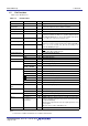
R8C/32D Group 4. 4. Special Function Registers (SFRs) Special Function Registers (SFRs) An SFR (special function register) is a control register for a peripheral function. Tables 4.1 to 4.8 list the special function registers and Table 4.9 lists the ID Code Areas and Option Function Select Area. Table 4.
R8C/32D Group Table 4.2 4.
R8C/32D Group Table 4.3 Address 0080h 0081h 0082h 0083h 0084h 0085h 0086h 0087h 0088h 0089h 008Ah 008Bh 008Ch 008Dh 008Eh 008Fh 0090h 0091h 0092h 0093h 0094h 0095h 0096h 0097h 0098h 0099h 009Ah 009Bh 009Ch 009Dh 009Eh 009Fh 00A0h 00A1h 00A2h 00A3h 00A4h 00A5h 00A6h 00A7h 00A8h 00A9h 00AAh 00ABh 00ACh 00ADh 00AEh 00AFh 00B0h 00B1h 00B2h 00B3h 00B4h 00B5h 00B6h 00B7h 00B8h 00B9h 00BAh 00BBh 00BCh 00BDh 00BEh 00BFh 4.
R8C/32D Group Table 4.4 4.
R8C/32D Group Table 4.5 Address 0100h 0101h 0102h 0103h 0104h 0105h 0106h 0107h 0108h 0109h 010Ah 010Bh 010Ch 010Dh 010Eh 010Fh 0110h 0111h 0112h 0113h 0114h 0115h 0116h 0117h 0118h 0119h 011Ah 011Bh 011Ch 011Dh 011Eh 011Fh 0120h 0121h 0122h 0123h 0124h 0125h 0126h 0127h 0128h 0129h 012Ah 012Bh 012Ch 012Dh 012Eh 012Fh 0130h 0131h 0132h 0133h 0134h 0135h 0136h 0137h 0138h 0139h 013Ah 013Bh 013Ch 013Dh 013Eh 013Fh Note: 1. 4.
R8C/32D Group Table 4.6 4. Special Function Registers (SFRs) SFR Information (6) (1) Address Register 0140h 0141h 0142h 0143h 0144h 0145h 0146h 0147h 0148h 0149h 014Ah 014Bh 014Ch 014Dh 014Eh 014Fh 0150h 0151h 0152h 0153h 0154h 0155h 0156h 0157h 0158h 0159h 015Ah 015Bh 015Ch 015Dh 015Eh 015Fh 0160h 0161h 0162h 0163h 0164h 0165h 0166h 0167h 0168h 0169h 016Ah 016Bh 016Ch 016Dh 016Eh 016Fh 0170h 0171h 0172h 0173h 0174h 0175h 0176h 0177h 0178h 0179h 017Ah 017Bh 017Ch 017Dh 017Eh 017Fh X: Undefined Note: 1.
R8C/32D Group Table 4.7 4.
R8C/32D Group Table 4.8 4.
R8C/32D Group 4. Special Function Registers (SFRs) Table 4.9 ID Code Areas and Option Function Select Area Address : FFDBh : FFDFh : FFE3h : FFEBh : FFEFh : FFF3h : FFF7h : FFFBh : FFFFh Area Name Notes: 1. 2.
R8C/32D Group 5. 5. Electrical Characteristics Electrical Characteristics Table 5.1 Absolute Maximum Ratings Symbol Parameter Rated Value Unit −0.3 to 6.5 V Input voltage −0.3 to VCC + 0.3 V VO Output voltage −0.3 to VCC + 0.3 V Pd Power dissipation 500 mW Topr Operating ambient temperature −20 to 85 (N version) / −40 to 85 (D version) °C Tstg Storage temperature −65 to 150 °C VCC/AVCC Supply voltage VI REJ03B0288-0100 Rev.1.
R8C/32D Group Table 5.2 5. Electrical Characteristics Recommended Operating Conditions Symbol Parameter Conditions Standard Min. Typ. Max. Unit VCC/AVCC Supply voltage 1.8 − 5.5 V VSS/AVSS Supply voltage − 0 − V 0.8 VCC − VCC V 0.5 VCC − VCC V 2.7 V ≤ VCC < 4.0 V 0.55 VCC − VCC V 1.8 V ≤ VCC < 2.7 V 0.65 VCC − VCC V 4.0 V ≤ VCC ≤ 5.5 V 0.65 VCC − VCC V 2.7 V ≤ VCC < 4.0 V 0.7 VCC − VCC V 1.8 V ≤ VCC < 2.7 V 0.8 VCC − VCC V 4.0 V ≤ VCC ≤ 5.5 V 0.
R8C/32D Group 5. Electrical Characteristics P1 P3 P4 Figure 5.1 30pF Ports P1, P3, P4 Timing Measurement Circuit REJ03B0288-0100 Rev.1.
R8C/32D Group Table 5.3 5. Electrical Characteristics A/D Converter Characteristics Symbol Parameter − Resolution − Absolute accuracy − Tolerance level impedance tCONV Conversion time Typ. Max. Unit − − 10 Bit AN8 to AN11 input − − ±3 LSB Vref = AVCC = 3.3 V AN8 to AN11 input − − ±5 LSB Vref = AVCC = 3.0 V AN8 to AN11 input − − ±5 LSB Vref = AVCC = 2.2 V AN8 to AN11 input − − ±5 LSB Vref = AVCC = 5.0 V AN8 to AN11 input − − ±2 LSB Vref = AVCC = 3.
R8C/32D Group Table 5.5 5. Electrical Characteristics Flash Memory (Program ROM) Electrical Characteristics Symbol Parameter Standard Conditions Min. Typ. Max. Unit 1,000 (3) − − times Byte program time − 80 500 µs − Block erase time − 0.
R8C/32D Group Table 5.6 5. Electrical Characteristics Voltage Detection 0 Circuit Electrical Characteristics Symbol Vdet0 Parameter Condition Standard Unit Min. Typ. Max. Voltage detection level Vdet0_0 (2) 1.80 1.90 2.05 V Voltage detection level Vdet0_1 (2) 2.15 2.35 2.50 V Voltage detection level Vdet0_2 (2) 2.70 2.85 3.05 V Voltage detection level Vdet0_3 (2) 3.55 3.80 4.
R8C/32D Group Table 5.8 5. Electrical Characteristics Voltage Detection 2 Circuit Electrical Characteristics Symbol Parameter Standard Condition At the falling of VCC Unit Min. Typ. Max. 3.70 4.00 4.30 V − 0.10 − V 150 µs Vdet2 Voltage detection level Vdet2_0 − Hysteresis width at the rising of Vcc in voltage detection 2 circuit − Voltage detection 2 circuit response time (2) At the falling of Vcc from 5 V to (Vdet2_0 − 0.
R8C/32D Group Table 5.10 5. Electrical Characteristics High-speed On-Chip Oscillator Circuit Electrical Characteristics Symbol − Parameter Standard Condition Unit Min. Typ. Max. VCC = 1.8 V to 5.5 V −20°C ≤ Topr ≤ 85°C 38.4 40 41.6 MHz VCC = 1.8 V to 5.5 V −40°C ≤ Topr ≤ 85°C 38.0 40 42.0 MHz High-speed on-chip oscillator frequency when the FRA4 register correction value is written into the FRA1 register and the FRA5 register correction value into the FRA3 register (3) VCC = 1.
R8C/32D Group Table 5.13 5. Electrical Characteristics Electrical Characteristics (1) [4.2 V ≤ Vcc ≤ 5.5 V] Symbol VOH Parameter Output “H” voltage Other than XOUT XOUT VOL Output “L” voltage Other than XOUT Hysteresis Unit Min. Typ. Max. Drive capacity High VCC = 5 V IOH = −20 mA VCC − 2.0 − VCC Drive capacity Low VCC = 5 V IOH = −5 mA VCC − 2.0 − VCC V 1.0 − VCC V VCC = 5V IOH = −200 µA V Drive capacity High VCC = 5 V IOL = 20 mA − − 2.
R8C/32D Group Table 5.14 Symbol ICC 5. Electrical Characteristics Electrical Characteristics (2) [3.3 V ≤ Vcc ≤ 5.5 V] (Topr = −20 to 85°C (N version) / −40 to 85°C (D version), unless otherwise specified.) Parameter Condition High-speed Power supply clock mode current (VCC = 3.3 to 5.5 V) Single-chip mode, output pins are open, other pins are VSS High-speed on-chip oscillator mode Low-speed on-chip oscillator mode Low-speed clock mode Wait mode Stop mode REJ03B0288-0100 Rev.1.
R8C/32D Group 5. Electrical Characteristics Timing Requirements (Unless Otherwise Specified: VCC = 5 V, VSS = 0 V at Topr = 25°C) Table 5.15 External Clock Input (XOUT, XCIN) Symbol Standard Parameter Min. Max.
R8C/32D Group Table 5.17 5. Electrical Characteristics Serial Interface Symbol Standard Parameter Min. Max.
R8C/32D Group Table 5.19 5. Electrical Characteristics Electrical Characteristics (3) [2.7 V ≤ Vcc < 4.2 V] Symbol VOH Parameter Output “H” voltage Other than XOUT Condition Other than XOUT VCC − 0.5 − VCC V − VCC V 1.0 − VCC V − − 0.5 V IOH = −200 µA Drive capacity High IOL = 5 mA IOL = 1 mA − − 0.5 V IOL = 200 µA − − 0.5 V VCC = 3.0 V INT0, INT1, INT3, KI0, KI1, KI2, KI3, TRAIO, TRBO, TRCIOA, TRCIOB, TRCIOC, TRCIOD, TRCTRG, TRCCLK, ADTRG, RXD0, RXD2, CLK0, CLK2 0.1 0.
R8C/32D Group Table 5.20 Symbol ICC 5. Electrical Characteristics Electrical Characteristics (4) [2.7 V ≤ Vcc < 3.3 V] (Topr = −20 to 85°C (N version) / −40 to 85°C (D version), unless otherwise specified.) Parameter Condition Power supply current High-speed (VCC = 2.7 to 3.3 V) clock mode Single-chip mode, output pins are open, other pins are VSS REJ03B0288-0100 Rev.1.
R8C/32D Group 5. Electrical Characteristics Timing requirements (Unless Otherwise Specified: VCC = 3 V, VSS = 0 V at Topr = 25°C) Table 5.21 External Clock Input (XOUT, XCIN) Symbol Standard Parameter Min. Max.
R8C/32D Group Table 5.23 5. Electrical Characteristics Serial Interface Symbol Standard Parameter Min. Max.
R8C/32D Group Table 5.25 5. Electrical Characteristics Electrical Characteristics (5) [1.8 V ≤ Vcc < 2.7 V] Symbol VOH Parameter Output “H” voltage Other than XOUT Condition Max. Drive capacity High IOH = −2 mA VCC − 0.5 − VCC IOH = −1 mA VCC − 0.5 − VCC V 1.0 − VCC V Drive capacity High IOL = 2 mA − − 0.5 V Drive capacity Low IOL = 1 mA − − 0.5 V IOL = 200 µA − − 0.5 V 0.05 0.2 − V 0.05 0.20 − V − − 4.
R8C/32D Group Table 5.26 Symbol ICC 5. Electrical Characteristics Electrical Characteristics (6) [1.8 V ≤ Vcc < 2.7 V] (Topr = −20 to 85°C (N version) / −40 to 85°C (D version), unless otherwise specified.) Parameter Condition Power supply current High-speed clock mode (VCC = 1.8 to 2.7 V) Single-chip mode, output pins are open, other pins are VSS REJ03B0288-0100 Rev.1.
R8C/32D Group 5. Electrical Characteristics Timing requirements (Unless Otherwise Specified: VCC = 2.2 V, VSS = 0 V at Topr = 25°C) Table 5.27 External Clock Input (XOUT, XCIN) Symbol Standard Parameter Min. Max.
R8C/32D Group Table 5.29 5. Electrical Characteristics Serial Interface Symbol Standard Parameter Min. Max. Unit tc(CK) CLKi input cycle time 800 − ns tW(CKH) CLKi input “H” width 400 − ns tW(CKL) CLKi input “L” width 400 − ns td(C-Q) TXDi output delay time − 200 ns th(C-Q) TXDi hold time 0 − ns tsu(D-C) RXDi input setup time 150 − ns th(C-D) RXDi input hold time 90 − ns i = 0, 2 VCC = 2.
R8C/32D Group Package Dimensions Package Dimensions Diagrams showing the latest package dimensions and mounting information are available in the “Packages” section of the Renesas Technology website. JEITA Package Code P-LSSOP20-4.4x6.5-0.65 RENESAS Code PLSP0020JB-A MASS[Typ.] 0.1g 11 *1 E 20 HE Previous Code 20P2F-A NOTE) 1. DIMENSIONS "*1" AND "*2" DO NOT INCLUDE MOLD FLASH. 2. DIMENSION "*3" DOES NOT INCLUDE TRIM OFFSET.
REVISION HISTORY R8C/32D Group Datasheet Description Rev. Date 0.01 Feb. 26, 2008 1.00 Feb. 26, 2010 All pages “Preliminary”, “Under development” deleted Page – 4 Summary First Edition issued Table 1.3 revised 22 to 41 “5. Electrical Characteristics” added All trademarks and registered trademarks are the property of their respective owners.
Sales Strategic Planning Div. Nippon Bldg., 2-6-2, Ohte-machi, Chiyoda-ku, Tokyo 100-0004, Japan Notes: 1. This document is provided for reference purposes only so that Renesas customers may select the appropriate Renesas products for their use.