
Datasheet


R8C/28 Group, R8C/29 Group 5. Electrical Characteristics
Rev.2.10 Sep 26, 2008 Page 47 of 67
REJ03B0169-0210
5.2 J, K Version
NOTES:
1. V
CC = 2.7 to 5.5 V at Topr = -40 to 85°C (J version) / -40 to 125°C (K version), unless otherwise specified.
2. The average output current indicates the average value of current measured during 100 ms.
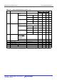
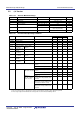
Table 5.34 Absolute Maximum Ratings
Symbol Parameter Condition Rated Value Unit
V
CC/AVCC Supply voltage -0.3 to 6.5 V
V
I Input voltage -0.3 to VCC + 0.3 V
V
O Output voltage -0.3 to VCC + 0.3 V
P
d Power dissipation -40 °C ≤ Topr ≤ 85 °C300mW
85
°C ≤ Topr ≤ 125 °C125mW
T
opr Operating ambient temperature -40 to 85 (J version) /
-40 to 125 (K version)
°C
T
stg Storage temperature -65 to 150 °C
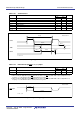
Table 5.35 Recommended Operating Conditions
Symbol Parameter Conditions
Standard
Unit
Min. Typ. Max.
V
CC/AVCC Supply voltage 2.7 − 5.5 V
V
SS/AVSS Supply voltage − 0 − V
V
IH Input “H” voltage 0.8 VCC − VCC V
V
IL Input “L” voltage 0 − 0.2 VCC V
I
OH(sum) Peak sum output
“H” current
Sum of all pins
I
OH(peak)
−−-60 mA
I
OH(peak) Peak output “H”
current
−−-10 mA
I
OH(avg) Average output
“H” current
−−-5 mA
I
OL(sum) Peak sum output
“L” currents
Sum of all pins
I
OL(peak)
−−60 mA
I
OL(peak) Peak output “L”
currents
−−10 mA
I
OL(avg) Average output
“L” current
−−5mA
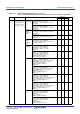
f
(XIN) XIN clock input oscillation frequency 3.0 V ≤ VCC ≤ 5.5 V (other than K
version)
0 − 20 MHz
3.0 V
≤ VCC ≤ 5.5 V (K version) 0 − 16 MHz
2.7 V
≤ VCC < 3.0 V 0 − 10 MHz
− System clock OCD2 = 0
XlN clock selected
3.0 V ≤ VCC ≤ 5.5 V (other than K
version)
0 − 20 MHz
3.0 V
≤ VCC ≤ 5.5 V (K version) 0 − 16 MHz
2.7 V
≤ VCC < 3.0 V 0 − 10 MHz
OCD2 = 1
On-chip oscillator
clock selected
FRA01 = 0
Low-speed on-chip oscillator clock
selected
− 125 − kHz
FRA01 = 1
High-speed on-chip oscillator clock
selected (other than K version)
−−20 MHz
FRA01 = 1
High-speed on-chip oscillator clock
selected
−−10 MHz