
Datasheet


R8C/28 Group, R8C/29 Group 5. Electrical Characteristics
Rev.2.10 Sep 26, 2008 Page 36 of 67
REJ03B0169-0210
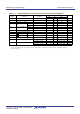
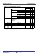
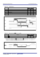
Table 5.17 Electrical Characteristics (3) [Vcc = 5 V]
(T
opr = -20 to 85°C (N version) / -40 to 85°C (D version), unless otherwise specified.)
Symbol Parameter Condition
Standard
Unit
Min. Typ. Max.
I
CC Power supply current
(V
CC = 3.3 to 5.5 V)
Single-chip mode,
output pins are open,
other pins are V
SS
Wait mode XIN clock off
High-speed on-chip oscillator off
Low-speed on-chip oscillator on = 125 kHz
While a WAIT instruction is executed
Peripheral clock operation
VCA27 = VCA26 = VCA25 = 0
VCA20 = 1
− 25 75 µA
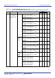
XIN clock off
High-speed on-chip oscillator off
Low-speed on-chip oscillator on = 125 kHz
While a WAIT instruction is executed
Peripheral clock off
VCA27 = VCA26 = VCA25 = 0
VCA20 = 1
− 23 60 µA
XIN clock off
High-speed on-chip oscillator off
Low-speed on-chip oscillator off
XCIN clock oscillator on = 32 kHz (high drive)
While a WAIT instruction is executed
VCA27 = VCA26 = VCA25 = 0
VCA20 = 1
− 4.0 −µA
XIN clock off
High-speed on-chip oscillator off
Low-speed on-chip oscillator off
XCIN clock oscillator on = 32 kHz (low drive)
While a WAIT instruction is executed
VCA27 = VCA26 = VCA25 = 0
VCA20 = 1
− 2.2 −µA
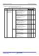
Stop mode XIN clock off, T
opr = 25°C
High-speed on-chip oscillator off
Low-speed on-chip oscillator off
CM10 = 1
Peripheral clock off
VCA27 = VCA26 = VCA25 = 0
− 0.8 3.0 µA
XIN clock off, T
opr = 85°C
High-speed on-chip oscillator off
Low-speed on-chip oscillator off
CM10 = 1
Peripheral clock off
VCA27 = VCA26 = VCA25 = 0
− 1.2 −µA