
Datasheet
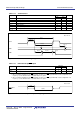


Table Of Contents
- 1. Overview
- 2. Central Processing Unit (CPU)
- 3. Memory
- 4. Special Function Registers (SFRs)
- 5. Electrical Characteristics
- Package Dimensions
A - 1
REVISION HISTORY R8C/18 Group, R8C/19 Group Datasheet
Rev. Date
Description
Page Summary
0.10 Nov 15, 2004 − First Edition issued
0.20 Jan 11, 2005 5, 6 Tables 1.3 and 1.4: The date updated
0.21 Apr 04, 2005 2, 3 Tables 1.1 and 1.2: Partly revised
4 Figure 1.1: Partly revised
5, 6 Tables 1.3 and 1.4: Partly revised
5, 6 Figure 1.2 and 1.3: Partly revised
7, 8 Figure 1.4 and 1.5: Partly revised
10 Table 1.6: Partly revised
16 Table 4.1: Partly revised
17 Table 4.2: Partly revised
18 Table 4.3: Partly revised
20 Package Dimensions are revised
1.00 May 27, 2005 5, 6 Tables 1.3 and 1.4: Partly revised
9 Table 1.5: Partly revised
25 Table 5.9: Revised
26 Table 5.10: Partly revised
28 Table 5.13: Partly revised
32 Table 5.20: Partly revised
1.10 Jun 09, 2005 26 Table 5.10: Partly revised
1.20 Nov 01, 2005 3 Table 1.2 Performance Outline of the R8C/19 Group;
Flash Memory: (Data area) → (Data flash)
(Program area) → (Program ROM) revised
4 Figure 1.1 Block Diagram;
“Peripheral Function” added,
“System Clock Generation” → “System Clock Generator” revised
6 Table 1.4 Product Information of R8C/19 Group;
ROM capacity: “Program area” → “Program ROM”,
“Data area” → “Data flash” revised
9 Table 1.5 Pin Description;
Power Supply Input: “VCC/AVCC” → “VCC”,
“VSS/AVSS” → “VSS” revised
Analog Power Supply Input: added
11 Figure 2.1 CPU Register;
“Reserved Area” → “Reserved Bit” revised
13 2.8.10 Reserved Area;
“Reserved Area” → “Reserved Bit” revised
15 3.2 R8C/19 Group, Figure 3.2 Memory Map of R8C/19 Group;
“Data area” → “Data flash”,
“Program area” → “Program ROM” revised