
Datasheet
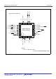


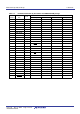

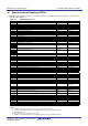
Table Of Contents
- 1. Overview
- 2. Central Processing Unit (CPU)
- 3. Memory
- 4. Special Function Registers (SFRs)
- 5. Electrical Characteristics
- Package Dimensions
R8C/18 Group, R8C/19 Group 1. Overview
Rev.1.40 Apr 14, 2006 Page 10 of 38
REJ03B0124-0140
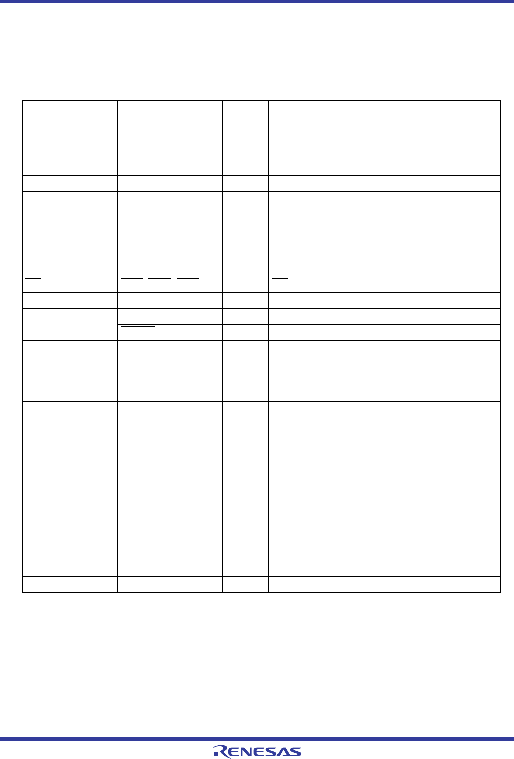
1.6 Pin Functions
Table 1.5 lists Pin Functions, Table 1.6 lists Pin Name Information by Pin Number of PLSP0020JB-A,
PRDP0020BA-A packages, and Table 1.7 lists Pin Name Information by Pin Number of PWQN0028KA-
B package.
I: Input O: Output I/O: Input and output
Table 1.5 Pin Functions
Type Symbol I/O Type Description
Power supply input VCC
VSS
I Apply 2.7 V to 5.5 V to the VCC pin. Apply 0 V to
the VSS pin.
Analog power
supply input
AVCC, AVSS I Power supply for the comparator
Connect a capacitor between AVCC and AVSS.
Reset input RESET
I Input “L” on this pin resets the MCU.
MODE MODE I Connect this pin to VCC via a resistor.
Main clock input XIN I These pins are provided for main clock generation
circuit I/O. Connect a ceramic resonator or a
crystal oscillator between the XIN and XOUT pins.
To use an external clock, input it to the XIN pin
and leave the XOUT pin open.
Main clock output XOUT O
INT
interrupt INT0, INT1, INT3 IINT interrupt input pins
Key input interrupt KI0
to KI3 I Key input interrupt input pins
Timer X CNTR0 I/O Timer X I/O pin
CNTR0
O Timer X output pin
Timer Z TZOUT O Timer Z output pin
Timer C TCIN I Timer C input pin
CMP0_0 to CMP0_2,
CMP1_0 to CMP1_2
O Timer C output pins
Serial interface CLK0 I/O Transfer clock I/O pin
RXD0, RXD1 I Serial data input pins
TXD0, TXD1 O Serial data output pins
Reference voltage
input
VREF I Reference voltage input pin to comparator
Comparator AN8 to AN11 I Analog input pins to comparator
I/O port P1_0 to P1_7, P3_3
to P3_5, P3_7, P4_5
I/O CMOS I/O ports. Each port has an I/O select
direction register, allowing each pin in the port to
be directed for input or output individually.
Any port set to input can be set to use a pull-up
resistor or not by a program.
P1_0 to P1_3 also function as LED drive ports.
Input port P4_2, P4_6, P4_7 I Input-only ports