To our customers, Old Company Name in Catalogs and Other Documents On April 1st, 2010, NEC Electronics Corporation merged with Renesas Technology Corporation, and Renesas Electronics Corporation took over all the business of both companies. Therefore, although the old company name remains in this document, it is a valid Renesas Electronics document. We appreciate your understanding. Renesas Electronics website: http://www.renesas.
Notice 1. 2. 3. 4. 5. 6. 7. All information included in this document is current as of the date this document is issued. Such information, however, is subject to change without any prior notice. Before purchasing or using any Renesas Electronics products listed herein, please confirm the latest product information with a Renesas Electronics sales office.
R8C/18 Group, R8C/19 Group SINGLE-CHIP 16-BIT CMOS MCU 1. REJ03B0124-0140 Rev.1.40 Apr 14, 2006 Overview These MCUs are fabricated using a high-performance silicon gate CMOS process, embedding the R8C/Tiny Series CPU core, and is packaged in a 20-pin molded-plastic LSSOP, SDIP or a 28-pin plastic molded-HWQFN. It implements sophisticated instructions for a high level of instruction efficiency. With 1 Mbyte of address space, they are capable of executing instructions at high speed.
R8C/18 Group, R8C/19 Group 1.2 1. Overview Performance Overview Table 1.1 outlines the Functions and Specifications for R8C/18 Group and Table 1.2 outlines the Functions and Specifications for R8C/19 Group. Table 1.1 Functions and Specifications for R8C/18 Group Item Specification CPU Number of fundamental 89 instructions instructions Minimum instruction execution 50 ns (f(XIN) = 20 MHz, VCC = 3.0 to 5.5 V) time 100 ns (f(XIN) = 10 MHz, VCC = 2.7 to 5.
R8C/18 Group, R8C/19 Group Table 1.2 1. Overview Functions and Specifications for R8C/19 Group Item Specification CPU Number of fundamental 89 instructions instructions Minimum instruction 50 ns (f(XIN) = 20 MHz, VCC = 3.0 to 5.5 V) execution time 100 ns (f(XIN) = 10 MHz, VCC = 2.7 to 5.5 V) Operation mode Single-chip Address space 1 Mbyte Memory capacity Refer to Table 1.
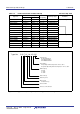
R8C/18 Group, R8C/19 Group 1.3 1. Overview Block Diagram Figure 1.1 shows a Block Diagram.
R8C/18 Group, R8C/19 Group 1.4 1. Overview Product Information Table 1.3 lists Product Information for R8C/18 Group and Table 1.4 lists Product Information for R8C/19 Group. Table 1.3 Product Information for R8C/18 Group Type No.
R8C/18 Group, R8C/19 Group Table 1.4 1. Overview Product Information for R8C/19 Group Type No.
R8C/18 Group, R8C/19 Group 1.5 1. Overview Pin Assignments Figure 1.4 shows Pin Assignments for PLSP0020JB-A Package (Top View), Figure 1.5 shows Pin Assignments for PRDP0020BA-A Package (Top View) and Figure 1.6 shows Pin Assignments for PWQN0028KA-B Package (Top View).
R8C/18 Group, R8C/19 Group 1. Overview PIN assignments (top view) 1 20 P3_4/CMP1_1 P3_7/CNTR0/TXD1 2 19 P3_3/TCIN/INT3/CMP1_0 RESET 3 18 P1_0/KI0/AN8/CMP0_0 XOUT/P4_7(1) 4 17 P1_1/KI1/AN9/CMP0_1 VSS/AVSS 5 16 P4_2/VREF XIN/P4_6 6 15 P1_2/KI2/AN10/CMP0_2 VCC/AVCC 7 14 P1_3/KI3/AN11/TZOUT MODE 8 13 P1_4/TXD0 P4_5/INT0/RXD1 9 12 P1_5/RXD0/CNTR01/INT11 10 11 P1_6/CLK0 P1_7/CNTR00/INT10 R8C/18 Group R8C/19 Group P3_5/CMP1_2 NOTE: 1. P4_7 is an input-only port.
NC NC NC P4_2/VREF NC PIN Assignment (top view) P1_3/AN11/KI3/TZOUT 1.
R8C/18 Group, R8C/19 Group 1.6 1. Overview Pin Functions Table 1.5 lists Pin Functions, Table 1.6 lists Pin Name Information by Pin Number of PLSP0020JB-A, PRDP0020BA-A packages, and Table 1.7 lists Pin Name Information by Pin Number of PWQN0028KAB package. Table 1.5 Pin Functions I/O Type Description Power supply input VCC VSS Type I Apply 2.7 V to 5.5 V to the VCC pin. Apply 0 V to the VSS pin.
R8C/18 Group, R8C/19 Group Table 1.6 Pin Number 1 2 3 4 5 6 7 8 9 1.
R8C/18 Group, R8C/19 Group Table 1.7 1.
R8C/18 Group, R8C/19 Group 2. 2. Central Processing Unit (CPU) Central Processing Unit (CPU) Figure 2.1 shows the CPU Registers. The CPU contains 13 registers. R0, R1, R2, R3, A0, A1, and FB configure a register bank. There are two sets of register bank.
R8C/18 Group, R8C/19 Group 2.1 2. Central Processing Unit (CPU) Data Registers (R0, R1, R2, and R3) R0 is a 16-bit register for transfer, arithmetic, and logic operations. The same applies to R1 to R3. R0 can be split into high-order bits (R0H) and low-order bits (R0L) to be used separately as 8-bit data registers. R1H and R1L are analogous to R0H and R0L. R2 can be combined with R0 and used as a 32-bit data register (R2R0). R3R1 is analogous to R2R0. 2.
R8C/18 Group, R8C/19 Group 2.8.7 2. Central Processing Unit (CPU) Interrupt Enable Flag (I) The I flag enables maskable interrupts. Interrupts are disabled when the I flag is set to 0, and are enabled when the I flag is set to 1. The I flag is set to 0 when an interrupt request is acknowledged. 2.8.8 Stack Pointer Select Flag (U) ISP is selected when the U flag is set to 0; USP is selected when the U flag is set to 1.
R8C/18 Group, R8C/19 Group 3. 3. Memory Memory 3.1 R8C/18 Group Figure 3.1 is a Memory Map of R8C/18 Group. The R8C/18 Group has 1 Mbyte of address space from addresses 00000h to FFFFFh. The internal ROM area is allocated lower addresses, beginning with address 0FFFFh. For example, a 16-Kbyte internal ROM is allocated addresses 0C000h to 0FFFFh. The fixed interrupt vector table is allocated addresses 0FFDCh to 0FFFFh. They store the starting address of each interrupt routine.
R8C/18 Group, R8C/19 Group 3.2 3. Memory R8C/19 Group Figure 3.2 is a Memory Map of R8C/19 Group. The R8C/19 group has 1 Mbyte of address space from addresses 00000h to FFFFFh. The internal ROM (program ROM) is allocated lower addresses, beginning with address 0FFFFh. For example, a 16-Kbyte internal ROM area is allocated addresses 0C000h to 0FFFFh. The fixed interrupt vector table is allocated addresses 0FFDCh to 0FFFFh. They store the starting address of each interrupt routine.
R8C/18 Group, R8C/19 Group 4. 4. Special Function Registers (SFRs) Special Function Registers (SFRs) An SFR (special function register) is a control register for a peripheral function. Tables 4.1 to 4.4 list the special function registers. Table 4.
R8C/18 Group, R8C/19 Group Table 4.2 Address 0040h 0041h 0042h 0043h 0044h 0045h 0046h 0047h 0048h 0049h 004Ah 004Bh 004Ch 004Dh 004Eh 004Fh 0050h 0051h 0052h 0053h 0054h 0055h 0056h 0057h 0058h 0059h 005Ah 005Bh 005Ch 005Dh 4.
R8C/18 Group, R8C/19 Group Table 4.3 Address 0080h 0081h 0082h 0083h 0084h 0085h 0086h 0087h 0088h 0089h 008Ah 008Bh 008Ch 008Dh 008Eh 008Fh 0090h 0091h 0092h 0093h 0094h 0095h 0096h 0097h 0098h 0099h 009Ah 009Bh 009Ch 009Dh 009Eh 009Fh 00A0h 00A1h 00A2h 00A3h 00A4h 00A5h 00A6h 00A7h 00A8h 00A9h 00AAh 00ABh 00ACh 00ADh 00AEh 00AFh 00B0h 00B1h 00B2h 00B3h 00B4h 00B5h 00B6h 00B7h 00B8h 00B9h 00BAh 00BBh 00BCh 00BDh 00BEh 00BFh 4.
R8C/18 Group, R8C/19 Group Table 4.4 Address 00C0h 00C1h 00C2h 00C3h 00C4h 00C5h 00C6h 00C7h 00C8h 00C9h 00CAh 00CBh 00CCh 00CDh 00CEh 00CFh 00D0h 00D1h 00D2h 00D3h 00D4h 00D5h 00D6h 00D7h 00D8h 00D9h 00DAh 00DBh 00DCh 00DDh 00DEh 00DFh 00E0h 00E1h 00E2h 00E3h 00E4h 00E5h 00E6h 00E7h 00E8h 00E9h 00EAh 00EBh 00ECh 00EDh 00EEh 00EFh 00F0h 00F1h 00F2h 00F3h 00F4h 00F5h 00F6h 00F7h 00F8h 00F9h 00FAh 00FBh 00FCh 00FDh 00FEh 00FFh 4.
R8C/18 Group, R8C/19 Group 5. 5. Electrical Characteristics Electrical Characteristics Table 5.1 Absolute Maximum Ratings Rated Value Unit VCC Symbol Supply voltage Parameter VCC = AVCC Condition -0.3 to 6.5 V AVCC Analog supply voltage VCC = AVCC -0.3 to 6.5 V V VI Input voltage -0.3 to VCC+0.3 VO Output voltage -0.3 to VCC+0.
R8C/18 Group, R8C/19 Group Table 5.3 5. Electrical Characteristics Comparator Characteristics Symbol Parameter Conditions − Resolution − Absolute accuracy φAD = 10 MHz(3) tconv Conversion time φAD = 10 MHz(3) Vref Reference voltage VIA Analog input voltage − Comparator conversion operating clock frequency(2) Standard Min. Typ. Max. Unit − − 1 Bit − − ±20 mV 1 − − µs 0 − AVCC V 0 − AVCC V 1 − 10 MHz NOTES: 1. VCC = 2.7 to 5.
R8C/18 Group, R8C/19 Group Table 5.4 Flash Memory (Program ROM) Electrical Characteristics Symbol − 5. Electrical Characteristics Parameter Program/erase endurance(2) Conditions Standard Unit Min. Typ. Max. R8C/18 Group 100(3) − − times R8C/19 Group 1,000(3) − − times µs − Byte program time − 50 400 − Block erase time − 0.
R8C/18 Group, R8C/19 Group Table 5.5 5. Electrical Characteristics Flash Memory (Data flash Block A, Block B) Electrical Characteristics Symbol Parameter Standard Conditions Min. Typ. Unit Max. 10,000(3) − − times Byte program time (Program/erase endurance ≤ 1,000 times) − 50 400 µs − Byte program time (Program/erase endurance > 1,000 times) − 65 − µs − Block erase time (Program/erase endurance ≤ 1,000 times) − 0.
R8C/18 Group, R8C/19 Group Table 5.6 5. Electrical Characteristics Voltage Detection 1 Circuit Electrical Characteristics Symbol Parameter Vdet1 Voltage detection level(3) − Voltage detection circuit self power consumption td(E-A) Waiting time until voltage detection circuit operation starts(2) Vccmin MCU operating voltage minimum value Condition VCA26 = 1, VCC = 5.0 V Standard Unit Min. Typ. Max. 2.70 2.85 3.00 V − 600 − nA − − 100 µs 2.7 − − V NOTES: 1.
R8C/18 Group, R8C/19 Group Table 5.8 5. Electrical Characteristics Reset Circuit Electrical Characteristics (When Using Voltage Monitor 1 Reset) Symbol Parameter Condition Standard Min. Power-on reset valid voltage Vpor2 tw(Vpor2-Vdet1) Supply voltage rising time when power-on reset is deasserted(1) Unit Typ. Max. -20°C ≤ Topr ≤ 85°C − − Vdet1 V -20°C ≤ Topr ≤ 85°C, tw(por2) ≥ 0s(3) − − 100 ms NOTES: 1. This condition is not applicable when using with Vcc ≥ 1.0 V. 2.
R8C/18 Group, R8C/19 Group Table 5.10 5. Electrical Characteristics High-speed On-Chip Oscillator Circuit Electrical Characteristics Symbol Parameter Condition Standard Min. Typ. Max. Unit − High-speed on-chip oscillator frequency when the reset is deasserted VCC = 5.0 V, Topr = 25 °C − 8 − MHz − High-speed on-chip oscillator frequency temperature supply voltage dependence(2) 0 to +60 °C/5 V ± 5 %(3) 7.76 − 8.24 MHz -20 to +85 °C/2.7 to 5.5 V(3) 7.68 − 8.32 MHz -40 to +85 °C/2.
R8C/18 Group, R8C/19 Group Table 5.12 Electrical Characteristics (1) [VCC = 5 V] Symbol VOH 5. Electrical Characteristics Parameter Output “H” voltage Except XOUT XOUT VOL Output “L” voltage Condition Standard Unit Min. Typ. Max. IOH = -5 mA VCC − 2.0 − VCC V IOH = -200 µA VCC − 0.3 − VCC V Drive capacity HIGH IOH = -1 mA VCC − 2.0 − VCC V Drive capacity LOW IOH = -500 µA VCC − 2.0 − VCC V Except P1_0 to P1_3, XOUT IOL = 5 mA − − 2.0 V IOL = 200 µA − − 0.
R8C/18 Group, R8C/19 Group Table 5.13 Symbol ICC 5. Electrical Characteristics Electrical Characteristics (2) [Vcc = 5 V] (Topr = -40 to 85 °C, unless otherwise specified.) Parameter Condition Unit Typ. Max.
R8C/18 Group, R8C/19 Group 5. Electrical Characteristics Timing Requirements (Unless Otherwise Specified: VCC = 5 V, VSS = 0 V at Ta = 25 °C) [VCC = 5 V] Table 5.14 XIN Input Symbol Standard Parameter Min. Max. Unit tc(XIN) XIN input cycle time 50 − ns tWH(XIN) XIN input “H” width 25 − ns tWL(XIN) XIN input “L” width 25 − ns VCC = 5 V tc(XIN) tWH(XIN) XIN input tWL(XIN) Figure 5.4 Table 5.
R8C/18 Group, R8C/19 Group Table 5.17 5. Electrical Characteristics Serial Interface Symbol Standard Parameter Min. Max.
R8C/18 Group, R8C/19 Group Table 5.19 Electrical Characteristics (3) [VCC = 3V] Symbol VOH VOL 5. Electrical Characteristics Parameter Output “H” voltage Output “L” voltage Hysteresis Standard Min. Typ. Max. Unit Except XOUT IOH = -1 mA VCC − 0.5 − VCC V XOUT Drive capacity HIGH IOH = -0.1 mA VCC − 0.5 − VCC V Drive capacity LOW IOH = -50 µA VCC − 0.5 − VCC V − − 0.5 V Except P1_0 to P1_3, XOUT IOL = 1mA P1_0 to P1_3 Drive capacity HIGH IOL = 2 mA − − 0.
R8C/18 Group, R8C/19 Group Table 5.20 Symbol ICC 5. Electrical Characteristics Electrical Characteristics (4) [Vcc = 3V] (Topr = -40 to 85 °C, unless otherwise specified.) Parameter Condition Unit Typ. Max.
R8C/18 Group, R8C/19 Group 5. Electrical Characteristics Timing requirements (Unless Otherwise Specified: VCC = 3 V, VSS = 0 V at Ta = 25 °C) [VCC = 3 V] Table 5.21 XIN Input Symbol Standard Parameter Min. Max. Unit tc(XIN) XIN input cycle time 100 − ns tWH(XIN) XIN input “H” width 40 − ns tWL(XIN) XIN input “L” width 40 − ns VCC = 3 V tc(XIN) tWH(XIN) XIN input tWL(XIN) Figure 5.9 Table 5.
R8C/18 Group, R8C/19 Group Table 5.24 5. Electrical Characteristics Serial Interface Symbol Standard Parameter Min. Max.
R8C/18 Group, R8C/19 Group Package Dimensions Package Dimensions JEITA Package Code P-LSSOP20-4.4x6.5-0.65 RENESAS Code PLSP0020JB-A Previous Code 20P2F-A 11 *1 E 20 HE MASS[Typ.] 0.1g NOTE) 1. DIMENSIONS "*1" AND "*2" DO NOT INCLUDE MOLD FLASH. 2. DIMENSION "*3" DOES NOT INCLUDE TRIM OFFSET. F 1 10 Index mark c A1 Reference Symbol D D E A2 A A1 bp c A L *2 A2 *3 e bp Detail F y HE e y L RENESAS Code PRDP0020BA-A Previous Code 20P4B Min 6.4 4.3 Nom Max 6.5 6.6 4.4 4.5 1.
R8C/18 Group, R8C/19 Group Package Dimensions JEITA Package Code RENESAS Code Previous Code MASS[Typ.] P-HWQFN28-5x5-0.50 PWQN0028KA-B 28PJW-B 0.05g D 15 21 22 21 15 14 14 22 E1 E D2 Lp 7 7 1 28 8 8 28 1 e bp x Reference Symbol F Dimension in Millimeters Min Nom Max D 4.9 5.0 5.1 E 4.9 5.0 5.1 A2 0.75 A A2 A y 0.8 A1 0 bp 0.15 A1 e Detail F Rev.1.40 Apr 14, 2006 REJ03B0124-0140 Page 38 of 38 Lp 0 0.05 0.2 0.25 0.5 0.5 0.6 0.7 x 0.05 y 0.
REVISION HISTORY R8C/18 Group, R8C/19 Group Datasheet Description Rev. Date 0.10 Nov 15, 2004 − 0.20 Jan 11, 2005 5, 6 Tables 1.3 and 1.4: The date updated 0.21 Apr 04, 2005 2, 3 Tables 1.1 and 1.2: Partly revised Page 4 1.00 May 27, 2005 Summary First Edition issued Figure 1.1: Partly revised 5, 6 Tables 1.3 and 1.4: Partly revised 5, 6 Figure 1.2 and 1.3: Partly revised 7, 8 Figure 1.4 and 1.5: Partly revised 10 Table 1.6: Partly revised 16 Table 4.
REVISION HISTORY Rev. Date 1.20 Nov 01, 2005 1.30 Dec 16, 2005 R8C/18 Group, R8C/19 Group Datasheet Description Page Summary 16 Table 4.1 SFR Information(1); 0009h: “XXXXXX00b” → “00h” 000Ah: “00XXX000b” → “00h” 001Eh: “XXXXX000b” → “00h” revised 18 Table 4.
Sales Strategic Planning Div. Nippon Bldg., 2-6-2, Ohte-machi, Chiyoda-ku, Tokyo 100-0004, Japan Keep safety first in your circuit designs! 1. Renesas Technology Corp. puts the maximum effort into making semiconductor products better and more reliable, but there is always the possibility that trouble may occur with them. Trouble with semiconductors may lead to personal injury, fire or property damage.