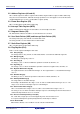
To our customers, Old Company Name in Catalogs and Other Documents On April 1st, 2010, NEC Electronics Corporation merged with Renesas Technology Corporation, and Renesas Electronics Corporation took over all the business of both companies. Therefore, although the old company name remains in this document, it is a valid Renesas Electronics document. We appreciate your understanding. Renesas Electronics website: http://www.renesas.
Notice 1. 2. 3. 4. 5. 6. 7. All information included in this document is current as of the date this document is issued. Such information, however, is subject to change without any prior notice. Before purchasing or using any Renesas Electronics products listed herein, please confirm the latest product information with a Renesas Electronics sales office.
R8C/13 Group SINGLE-CHIP 16-BIT CMOS MICROCOMPUTER REJ03B0069-0120 Rev.1.20 Jan 27, 2006 1. Overview This MCU is built using the high-performance silicon gate CMOS process using a R8C/Tiny Series CPU core and is packaged in a 32-pin plastic molded LQFP. This MCU operates using sophisticated instructions featuring a high level of instruction efficiency. With 1M bytes of address space, it is capable of executing instructions at high speed. The data flash ROM (2 KB X 2 blocks) is embedded. 1.
R8C/13 Group 1. Overview 1.2 Performance Overview Table 1.1. lists the performance outline of this MCU. Table 1.1 Performance outline Item Performance CPU Number of basic instructions 89 instructions Minimum instruction execution time 50 ns (f(XIN) = 20 MHZ, VCC = 3.0 to 5.5 V) 100 ns (f(XIN) = 10 MHZ, VCC = 2.7 to 5.5 V) Operating mode Single-chip Address space 1M bytes Memory capacity See Table 1.2.
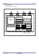
R8C/13 Group 1. Overview 1.3 Block Diagram Figure 1.1 shows this MCU block diagram.
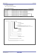
R8C/13 Group 1. Overview 1.4 Product Information Table 1.2 lists the product information. Table 1.2 Product Information As of January 2006 ROM capacity Type No.
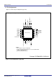
R8C/13 Group 1. Overview 1.5 Pin Assignments Figure 1.3 shows the pin configuration (top view).
R8C/13 Group 1. Overview 1.6 Pin Description Table 1.3 shows the pin description Table 1.3 Pin description Signal name Power supply input IVcc Pin name Vcc, Vss IVcc I/O type O Analog power supply input AVcc, AVss I Power supply input pins for A/D converter. Connect the AVcc pin to Vcc. Connect the AVss pin to Vss. Connect a capacitor between pins AVcc and AVss. Reset input CNVss MODE Main clock input RESET CNVss MODE XIN I I I I I ___________ Function Apply 2.7 V to 5.5 V to the Vcc pin.
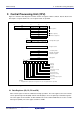
R8C/13 Group 2. Central Processing Unit (CPU) 2. Central Processing Unit (CPU) Figure 2.1 shows the CPU Register. The CPU contains 13 registers. Of these, R0, R1, R2, R3, A0, A1 and FB comprise a register bank. Two sets of register banks are provided.
R8C/13 Group 2. Central Processing Unit (CPU) 2.2 Address Registers (A0 and A1) A0 is a 16-bit register for address register indirect addressing and address register relative addressing. They also are used for transfer, arithmetic and logic operations. The same applies to A1 as A0. A0 can be combined with A0 to be used as a 32-bit address register (A1A0). 2.3 Frame Base Register (FB) FB is a 16-bit register for FB relative addressing. 2.
R8C/13 Group 3. Memory 3. Memory Figure 3.1 is a memory map of this MCU. This MCU provides 1-Mbyte address space from addresses 0000016 to FFFFF16. The internal ROM (program ROM) is allocated lower addresses beginning with address 0FFFF16. For example, a 16-Kbyte internal ROM is allocated addresses from 0C00016 to 0FFFF16. The fixed interrupt vector table is allocated addresses 0FFDC16 to 0FFFF16. They store the starting address of each interrupt routine.
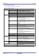
R8C/13 Group 4. Special Function Register (SFR) 4. Special Function Register (SFR) SFR(Special Function Register) is the control register of peripheral functions. Tables 4.1 to 4.4 list the SFR information Table 4.
R8C/13 Group 4. Special Function Register (SFR) Table 4.
R8C/13 Group 4. Special Function Register (SFR) Table 4.
R8C/13 Group 4. Special Function Register (SFR) Table 4.
R8C/13 Group 5. Electrical Characteristics 5. Electrical Characteristics Table 5.1 Absolute Maximum Ratings Condition Rated value Unit VCC Symbol Supply voltage Parameter VCC=AVCC -0.3 to 6.5 V AVCC Analog supply voltage VCC=AVCC -0.3 to 6.5 V VI Input voltage -0.3 to VCC+0.3 V VO Output voltage -0.3 to VCC+0.3 V Pd Power dissipation 300 mW Topr Operating ambient temperature -20 to 85 / -40 to 85 (D version) C Tstg Storage temperature Topr=25 C C -65 to 150 Table 5.
R8C/13 Group 5. Electrical Characteristics Table 5.3 A/D Conversion Characteristics Symbol Parameter – Resolution – Absolute accuracy RLADDER tCONV VREF VIA Ladder resistance Conversion time Measuring condition Standard Unit Min. Typ. Max. Vref =VCC 10 Bit 10 bit mode øAD=10 MHz, Vref=Vcc=5.0V ±3 LSB 8 bit mode øAD=10 MHz, Vref=Vcc=5.0V ±2 LSB 10 bit mode øAD=10 MHz, Vref=Vcc=3.3V(3) ±5 LSB 8 bit mode Vref=Vcc=3.
R8C/13 Group 5. Electrical Characteristics Table 5.4 Flash Memory (Program ROM) Electrical Characteristics Symbol Parameter Measuring condition Min. Standard Typ. Max Unit times – – Program/Erase endurance(2) Byte program time 50 µs – Block erase time 0.4 s td(SR-ES) 1000(3) 8 Time delay from Suspend Request until Erase Suspend ms – Erase Suspend Request Interval 10 – Program, Erase Voltage 2.7 5.5 V – – Read Voltage 2.7 5.
R8C/13 Group 5. Electrical Characteristics Table 5.5 Flash Memory (Data flash Block A, Block B) Electrical Characteristics(4) Symbol Parameter Standard Min. Typ. Measuring condition Program/Erase endurance(2) – Byte program time(program/erase endurance ≤1000 times) 50 – Byte program time(program/erase endurance >1000 times) 65 – Block erase time(program/erase endurance ≤1000 times) Block erase time(program/erase endurance >1000 times) 0.2 td(SR-ES) – – – – – 10000(3) 400 µs µs 9 0.
R8C/13 Group 5. Electrical Characteristics Table 5.6 Voltage Detection Circuit Electrical Characteristics Symbol Vdet Measuring condition Parameter Voltage detection level Min. Voltage detection interrupt request generating time(2) Microcomputer operation voltage minimum value Unit V µs nA 600 VC27=1, VCC=5.0V Vccmin 4.3 40 Voltage detection circuit self consumption current Waiting time until voltage detection circuit operation starts(3) Max. 3.8 3.3 td(E-A) Standard Typ. 20 µs V 2.
R8C/13 Group 5. Electrical Characteristics Table 5.9 High-speed On-Chip Oscillator Circuit Electrical Characteristics Symbol Measuring condition Parameter High-speed on-chip oscillator frequency 1 / {td(HRoffset)+td(HR)} when the reset is released td(HRoffset) Settable high-speed on-chip oscillator minimum period td(HR) Min. VCC=5.0V, Topr=25 °C Set "4016" in the HR1 register VCC=5.
R8C/13 Group 5. Electrical Characteristics Table 5.12 Electrical Characteristics (2) Symbol [Vcc=5V] Measuring condition Parameter High-speed mode Medium-speed mode ICC Power supply current (VCC=3.3 to 5.
R8C/13 Group 5. Electrical Characteristics Timing requirements [VCC=5V] (Unless otherwise noted: VCC = 5V, VSS = 0V at Topr = 25 °C) Table 5.13 XIN input Symbol tC(XIN) tWH(XIN) tWL(XIN) Parameter XIN input cycle time XIN input HIGH pulse width XIN input LOW pulse width Standard Min. Max. 50 – 25 – 25 – Unit Standard Min. Max. 100 – 40 – 40 – Unit Standard Min. Max. 400(1) – 200(2) – 200(2) – Unit Standard Min. Max. 200 – 100 – 100 – 80 – 0 – 35 – 90 – Unit Standard Min. Max.
R8C/13 Group 5. Electrical Characteristics VCC = 5V tc(CNTR0) tWH(CNTR0) CNTR0 input tWL(CNTR0) tc(TCIN) tWH(TCIN) TCIN input tWL(TCIN) tc(XIN) tWH(XIN) XIN input tWL(XIN) tc(CK) tW(CKH) CLKi tW(CKL) th(C-Q) TxDi td(C-Q) tsu(D-C) RxDi tW(INL) INTi tW(INH) Figure 5.4 Vcc=5V timing diagram Rev.1.
R8C/13 Group 5. Electrical Characteristics Table 5.18 Electrical Characteristics (3) Symbol [Vcc=3V] Measuring condition Parameter "H" output voltage VOH "L" output voltage VOL Except XOUT IOH=-1mA XOUT Drive capacity HIGH Drive capacity LOW Except P10 to P17, XOUT IOL= 1 mA P10 to P17 Drive capacity HIGH Drive capacity LOW XOUT Drive capacity HIGH Drive capacity LOW VT+-VT- Hysteresis II H "H" input current Min. VCC-0.5 V 0 .5 V IOL= 2 mA IOL= 1 mA 0 .5 V 0 .5 V IOL= 0.
R8C/13 Group 5. Electrical Characteristics Table 5.19 Electrical Characteristics (4) Symbol [Vcc=3V] Measuring condition Parameter High-speed mode Medium-speed mode ICC Power supply current (VCC=2.7 to 3.
R8C/13 Group 5. Electrical Characteristics Timing requirements [VCC=3V] (Unless otherwise noted: VCC = 3V, VSS = 0V at Topr = 25 °C) Table 5.20 XIN input Symbol tC(XIN) tWH(XIN) tWL(XIN) Parameter XIN input cycle time XIN input HIGH pulse width XIN input LOW pulse width Standard Min. Max. 100 – 40 – 40 – Unit Standard Min. Max. 300 – 120 – 120 – Unit Standard Min. Max. 1200(1) – 600(2) – 600(2) – Unit Standard Min. Max. 300 – 150 – 150 – 160 – 0 – 55 – 90 – Unit Standard Min. Max.
R8C/13 Group 5. Electrical Characteristics VCC = 3V tc(CNTR0) tWH(CNTR0) CNTR0 input tWL(CNTR0) tc(TCIN) tWH(TCIN) TCIN input tWL(TCIN) tc(XIN) tWH(XIN) XIN input tWL(XIN) tc(CK) tW(CKH) CLKi tW(CKL) th(C-Q) TxDi td(C-Q) tsu(D-C) RxDi tW(INL) INTi tW(INH) Figure 5.5 Vcc=3V timing diagram Rev.1.
R8C/13 Group Package Dimensions Package Dimensions JEITA Package Code P-LQFP32-7x7-0.80 RENESAS Code PLQP0032GB-A Previous Code 32P6U-A MASS[Typ.] 0.2g HD *1 D 24 17 NOTE) 1. DIMENSIONS "*1" AND "*2" DO NOT INCLUDE MOLD FLASH. 2. DIMENSION "*3" DOES NOT INCLUDE TRIM OFFSET. 16 25 bp c c1 HE *2 E b1 Reference Symbol 9 1 ZE Terminal cross section 32 8 ZD c A A1 F A2 Index mark L D E A2 HD HE A A1 bp b1 c c1 L1 y e Rev.1.
REVISION HISTORY Rev. R8C/13 Group Datasheet Date Description Summary Page First edition issued 0.10 Oct 28, 2003 0.20 Dec05, 2003 5 Figure 1.3 revised 10 Chapter 4, NOTES revised 16 Table 5.4 revised Table 5.5 revised 17 Table 5.6 revised Figure 5.3 added 18 Table 5.8 revised Table 5.10 revised 21 Figure 5.3 revised to Figure 5.4 22 Table 5.17 revised 25 Figure 5.4 revised to Figure 5.5 1.
REVISION HISTORY Rev. R8C/13 Group Datasheet Date Description Summary Page 1.10 Apr.27.2005 17 18 22 26 Table 5.7, 5.8 revised Table 5.10, Table 5.11 partly revised Table 5.18 partly revised Package Dimensions revised 1.20 Jan.27.2006 2 3 4 Table 1.1 Performance outline revised Figure 1.1 Block diagram partly revised 1.4 Product Information, title of Table 1.2 “Product List” → “Product Informaton” revised ROM capacity; “Program area” → “Program ROM”, “Data area” → “Data flash” revised Figure 1.
REVISION HISTORY Rev. R8C/13 Group Datasheet Date Description Summary Page 1.20 Jan.27.2006 20 23 24 Table 5.12 Electrical Characteristics (2) [VCC=5V]; NOTES: 1, 2 revised Measuring condition Stop mode: “Topr=-25 °C” added Table 5.18 Electrical Characteristics (3) [VCC=3V] “P10 to P17 Except XOUT” → “Except P10 to P17, XOUT” revised Table 5.
Sales Strategic Planning Div. Nippon Bldg., 2-6-2, Ohte-machi, Chiyoda-ku, Tokyo 100-0004, Japan Keep safety first in your circuit designs! 1. Renesas Technology Corp. puts the maximum effort into making semiconductor products better and more reliable, but there is always the possibility that trouble may occur with them. Trouble with semiconductors may lead to personal injury, fire or property damage.