
Datasheet


RL78/L12
CHAPTER 31 ELECTRICAL SPECIFICATIONS (G: TA = -40 to +105°C)
R01UH0330EJ0200 Rev.2.00 957
Dec 13, 2013
31.7.2 Internal voltage boosting method
(1) 1/3 bias method
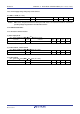
(T
A = −40 to +105°C, 2.4 V ≤ VDD ≤ 5.5 V, VSS = 0 V)
Parameter Symbol Conditions MIN. TYP. MAX. Unit
LCD output voltage variation range VL1 C1 to C4
Note 1
= 0.47
μ
F
VLCD = 04H 0.90 1.00
1.08
V
VLCD = 05H 0.95 1.05
1.13
V
VLCD = 06H 1.00 1.10
1.18
V
VLCD = 07H 1.05 1.15
1.23
V
VLCD = 08H 1.10 1.20
1.28
V
VLCD = 09H 1.15 1.25
1.33
V
VLCD = 0AH 1.20 1.30
1.38
V
VLCD = 0BH 1.25 1.35
1.43
V
VLCD = 0CH 1.30 1.40
1.48
V
VLCD = 0DH 1.35 1.45
1.53
V
VLCD = 0EH 1.40 1.50
1.58
V
VLCD = 0FH 1.45 1.55
1.63
V
VLCD = 10H 1.50 1.60
1.68
V
VLCD = 11H 1.55 1.65
1.73
V
VLCD = 12H 1.60 1.70
1.78
V
VLCD = 13H 1.65 1.75
1.83
V
Doubler output voltage VL2 C1 to C4
Note 1
= 0.47
μ
F 2 VL1
−0.1
2 V
L1 2 VL1 V
Tripler output voltage VL4 C1 to C4
Note 1
= 0.47
μ
F 3 VL1
−0.15
3 V
L1 3 VL1 V
Reference voltage setup time
Note 2
tVWAIT1 5 ms
Voltage boost wait time
Note 3
tVWAIT2 C1 to C4
Note 1
= 0.47
μ
F 500 ms
Notes 1. This is a capacitor that is connected between voltage pins used to drive the LCD.
C1: A capacitor connected between CAPH and CAPL
C2: A capacitor connected between V
L1 and GND
C3: A capacitor connected between V
L2 and GND
C4: A capacitor connected between VL4 and GND
C1 = C2 = C3 = C4 = 0.47 μF±30%
2. This is the time required to wait from when the reference voltage is specified by using the VLCD register (or
when the internal voltage boosting method is selected [by setting the MDSET1 and MDSET0 bits of the
LCDM0 register to 01B] if the default value reference voltage is used) until voltage boosting starts (VLCON = 1).
3. This is the wait time from when voltage boosting is started (VLCON = 1) until display is enabled (LCDON = 1).