
Datasheet


RL78/L12 CHAPTER 30 ELECTRICAL SPECIFICATIONS (A, G: T
A = -40 to +85°C)
R01UH0330EJ0200 Rev.2.00 863
Dec 13, 2013
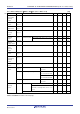
(TA = −40 to +85°C, 1.6 V ≤ EVDD = VDD ≤ 5.5 V, VSS = EVSS = 0 V) (5/5)
Items Symbol Conditions MIN. TYP. MAX. Unit
Input leakage
current, high
I
LIH1
P10 to P17, P30 to P32,
P40 to P43, P50 to P54, P60,
P61, P70 to P74, P120,
P125 to P127, P140 to P147
VI = EVDD 1
μ
A
ILIH2 P20, P21, P137, RESET VI = VDD 1
μ
A
ILIH3
P121 to P124
(X1, X2, XT1, XT2, EXCLK,
EXCLKS)
V
I = VDD
In input port or
external clock
input
1
μ
A
In resonator
connection
10
μ
A
Input leakage
current, low
I
LIL1
P10 to P17, P30 to P32,
P40 to P43, P50 to P54, P60,
P61, P70 to P74, P120,
P125 to P127, P140 to P147
VI = EVSS −1
μ
A
ILIL2 P20, P21, P137, RESET VI = VSS −1
μ
A
ILIL3
P121 to P124
(X1, X2, XT1, XT2, EXCLK,
EXCLKS)
V
I = VSS
In input port or
external clock
input
−1
μ
A
In resonator
connection
−10
μ
A
On-chip pll-up
resistance
R
U1 VI = EVSS SEGxx port
2.4 V
≤
EV
DD
= V
DD
≤
5.5 V
10 20 100 kΩ
1.6 V
≤
EV
DD
= V
DD
< 2.4 V
10 30 100 kΩ
RU2 Ports other than above
(Except for P60, P61, and
P130)
10 20 100 kΩ
Remark Unless specified otherwise, the characteristics of alternate-function pins are the same as those of the port
pins.