
Datasheet


RL78/L12
CHAPTER 31 ELECTRICAL SPECIFICATIONS (G: TA = -40 to +105°C)
R01UH0330EJ0200 Rev.2.00 951
Dec 13, 2013
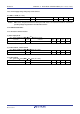
(2) When reference voltage (+) = AVREFP/ANI0 (ADREFP1 = 0, ADREFP0 = 1), reference voltage (−) = AVREFM/ANI1
(ADREFM = 1), target pin : ANI16 to ANI23
(T
A = −40 to +105°C, 2.4 V ≤ EVDD = VDD ≤ 5.5 V, 2.4 V ≤ AVREFP ≤ VDD ≤ 5.5 V, VSS = EVSS = 0 V, Reference voltage (+)
= AVREFP, Reference voltage (−) = AVREFM = 0 V)
Parameter Symbol Conditions MIN. TYP. MAX. Unit
Resolution RES 8 10 bit
Overall error
Note 1
AINL
10-bit resolution
AV
REFP = EVDD = VDD
Note 3
2.4 V ≤ AV
REFP ≤ 5.5 V 1.2 ±5.0 LSB
Conversion time tCONV
10-bit resolution
AV
REFP = EVDD = VDD
Note 3
3.6 V ≤ V
DD ≤ 5.5 V 2.125 39
μ
s
2.7 V ≤ VDD ≤ 5.5 V 3.1875 39
μ
s
2.4 V ≤ VDD ≤ 5.5 V 17 39
μ
s
Zero-scale error
Notes 1, 2
EZS
10-bit resolution
AV
REFP = EVDD = VDD
Note 3
2.4 V ≤ AV
REFP ≤ 5.5 V ±0.35 %FSR
Full-scale error
Notes 1, 2
EFS
10-bit resolution
AV
REFP = EVDD = VDD
Note 3
2.4 V ≤ AV
REFP ≤ 5.5 V ±0.35 %FSR
Integral linearity error
Note 1
ILE
10-bit resolution
AV
REFP = EVDD = VDD
Note 3
2.4 V ≤ AV
REFP ≤ 5.5 V ±3.5 LSB
Differential linearity error
Note 1
DLE
10-bit resolution
AV
REFP = EVDD = VDD
Note 3
2.4 V ≤ AV
REFP ≤ 5.5 V ±2.0 LSB
Analog input voltage VAIN ANI16 to ANI23 0
AV
REFP
and EV
DD
V
Notes 1. Excludes quantization error (±1/2 LSB).
2. This value is indicated as a ratio (%FSR) to the full-scale value.
3. When AV
REFP < EVDD = VDD, the MAX. values are as follows.
Overall error: Add ±4.0 LSB to the MAX. value when AV
REFP = VDD.
Zero-scale error/Full-scale error: Add ±0.20%FSR to the MAX. value when AVREFP = VDD.
Integral linearity error/ Differential linearity error: Add ±2.0 LSB to the MAX. value when AV
REFP = VDD.