
Datasheet


RL78/G12 3. ELECTRICAL SPECIFICATIONS (G: T
A = −40 to +105°C)
R01DS0193EJ0200 Rev.2.00
Sep 06, 2013
Page 94 of 106
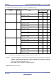
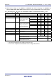
3.5.2 Serial interface IICA
(TA = −40 to +105°C, 2.4 V ≤ VDD ≤ 5.5 V, VSS = 0 V)
Parameter Symbol Conditions HS (high-speed main) mode Unit
Standard Mode Fast Mode
MIN. MAX. MIN. MAX.
SCLA0 clock frequency fSCL Fast mode: fCLK ≥ 3.5 MHz 0 400 kHz
Normal mode: fCLK ≥ 1 MHz 0 100 kHz
Setup time of restart condition tSU:STA 4.7 0.6
μ
s
Hold time
Note 1
tHD:STA 4.0 0.6
μ
s
Hold time when SCLA0 = “L” tLOW 4.7 1.3
μ
s
Hold time when SCLA0 = “H” tHIGH 4.0 0.6
μ
s
Data setup time (reception) tSU:DAT 250 100 ns
Data hold time (transmission)
Note 2
tHD:DAT 0 3.45 0 0.9
μ
s
Setup time of stop condition tSU:STO 4.0 0.6
μ
s
Bus-free time tBUF 4.7 1.3
μ
s
Notes 1. The first clock pulse is generated after this period when the start/restart condition is detected.
2. The maximum value (MAX.) of t
HD:DAT is during normal transfer and a wait state is inserted in the ACK
(acknowledge) timing.
Caution Only in the 30-pin products, the values in the above table are applied even when bit 2 (PIOR2) in the
peripheral I/O redirection register (PIOR) is 1. At this time, the pin characteristics (I
OH1, IOL1, VOH1,
V
OL1) must satisfy the values in the redirect destination.
Remark The maximum value of C
b (communication line capacitance) and the value of Rb (communication line pull-up
resistor) at that time in each mode are as follows.
Normal mode: C
b = 400 pF, Rb = 2.7 kΩ
Fast mode: C
b = 320 pF, Rb = 1.1 kΩ
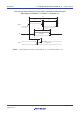
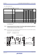
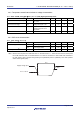
IICA serial transfer timing
tLOW tR
tHIGH tF
tBUF
tHD:DAT
tSU:DAT
tHD:STA
tSU:STA tHD:STA tSU:STO
SCLA0
SDAA0
Stop
condition
Start
condition
Restart
condition
Stop
condition