
Datasheet


RL78/G12 3. ELECTRICAL SPECIFICATIONS (G: T
A = −40 to +105°C)
R01DS0193EJ0200 Rev.2.00
Sep 06, 2013
Page 92 of 106
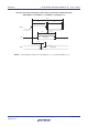
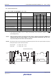
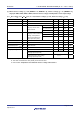
(8) Communication at different potential (1.8 V, 2.5 V, 3 V) (simplified I
2
C mode)
(TA = −40 to +105°C, 2.4 V ≤ VDD ≤ 5.5 V, VSS = 0 V)
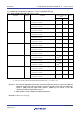
Parameter Symbol Conditions
HS (high-speed main)
Mode
Unit
MIN. MAX.
SCLr clock frequency fSCL
4.0 V ≤ V
DD ≤ 5.5 V, 2.7 V ≤ Vb ≤ 4.0 V,
C
b = 100 pF, Rb = 2.8 kΩ
100
Note1
kHz
2.7 V ≤ VDD < 4.0 V, 2.3 V ≤ Vb ≤ 2.7 V,
C
b = 100 pF, Rb = 2.7 kΩ
100
Note1
kHz
2.4 V ≤ VDD < 3.3 V, 1.6 V ≤ Vb ≤ 2.0 V,
C
b = 100 pF, Rb = 5.5 kΩ
100
Note1
kHz
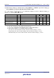
Hold time when SCLr = “L” tLOW
4.0 V ≤ V
DD ≤ 5.5 V, 2.7 V ≤ Vb ≤ 4.0 V,
C
b = 100 pF, Rb = 2.8 kΩ
4600 ns
2.7 V ≤ VDD < 4.0 V, 2.3 V ≤ Vb ≤ 2.7 V,
C
b = 100 pF, Rb = 2.7 kΩ
4600 ns
2.4 V ≤ VDD < 3.3 V, 1.6 V ≤ Vb ≤ 2.0 V,
C
b = 100 pF, Rb = 5.5 kΩ
4650 ns
Hold time when SCLr = “H” tHIGH
4.0 V ≤ V
DD ≤ 5.5 V, 2.7 V ≤ Vb ≤ 4.0 V,
C
b = 100 pF, Rb = 2.8 kΩ
2700 ns
2.7 V ≤ VDD < 4.0 V, 2.3 V ≤ Vb ≤ 2.7 V,
C
b = 100 pF, Rb = 2.7 kΩ
2400 ns
2.4 V ≤ VDD < 3.3 V, 1.6 V ≤ Vb ≤ 2.0 V,
C
b = 100 pF, Rb = 5.5 kΩ
1830 ns
Data setup time (reception) tSU:DAT
4.0 V ≤ V
DD ≤ 5.5 V, 2.7 V ≤ Vb ≤ 4.0 V,
C
b = 100 pF, Rb = 2.8 kΩ
1/f
MCK
+ 760
Note3
ns
2.7 V ≤ VDD < 4.0 V, 2.3 V ≤ Vb ≤ 2.7 V,
C
b = 100 pF, Rb = 2.7 kΩ
1/f
MCK
+ 760
Note3
ns
2.4 V ≤ VDD < 3.3 V, 1.6 V ≤ Vb ≤ 2.0 V,
C
b = 100 pF, Rb = 5.5 kΩ
1/f
MCK
+ 570
Note3
ns
Data hold time (transmission) tHD:DAT
4.0 V ≤ V
DD ≤ 5.5 V, 2.7 V ≤ Vb ≤ 4.0 V,
C
b = 100 pF, Rb = 2.8 kΩ
0 1420 ns
2.7 V ≤ VDD < 4.0 V, 2.3 V ≤ Vb ≤ 2.7 V,
C
b = 100 pF, Rb = 2.7 kΩ
0 1420 ns
2.4 V ≤ VDD < 3.3 V, 1.6 V ≤ Vb ≤ 2.0 V,
C
b = 100 pF, Rb = 5.5 kΩ
0 1215 ns
Notes 1. The value must also be equal to or less than fMCK/4.
2. Set t
SU:DAT so that it will not exceed the hold time when SCLr = "L" or SCLr = "H".
Cautions 1. Select the TTL input buffer and the N-ch open drain output (V
DD tolerance) mode for the SDAr pin
and the N-ch open drain output (V
DD tolerance) mode for the SCLr pin by using port input mode
register 1 (PIM1) and port output mode register 1 (POM1). For VIH and VIL, see the DC
characteristics with TTL input buffer selected.
2. IIC01 and IIC11 cannot communicate at different potential.
(Remarks are listed on the next page.)