
Datasheet


RL78/G12 2. ELECTRICAL SPECIFICATIONS (A, D: T
A = −40 to +85°C)
R01DS0193EJ0200 Rev.2.00
Sep 06, 2013
Page 24 of 106
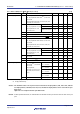
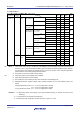
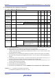
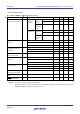
(1) 20-, 24-pin products
(TA = −40 to +85°C, 1.8 V ≤ VDD ≤ 5.5 V, VSS = 0 V) (2/2)
Parameter Symbol Conditions MIN. TYP. MAX. Unit
Supply
current
Note 1
I
DD2
Note 2
HALT
mode
HS (High-speed
main) mode
Note 6
f
IH = 24 MHz
Note 4
VDD = 5.0 V 440 1210
μ
A
VDD = 3.0 V 440 1210
fIH = 16 MHz
Note 4
VDD = 5.0 V 400 950
μ
A
VDD = 3.0 V 400 950
LS (Low-speed
main) mode
Note 6
f
IH = 8 MHz
Note 4
VDD = 3.0 V 270 542
μ
A
VDD = 2.0 V 270 542
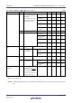
HS (High-speed
main) mode
Note 6
f
MX = 20 MHz
Note 3
,
V
DD = 5.0 V
Square wave input 280 1000
μ
A
Resonator connection 450 1170
fMX = 20 MHz
Note 3
,
V
DD = 3.0 V
Square wave input 280 1000
μ
A
Resonator connection 450 1170
fMX = 10 MHz
Note 3
,
V
DD = 5.0 V
Square wave input 190 590
μ
A
Resonator connection 260 660
fMX = 10 MHz
Note 3
,
V
DD = 3.0 V
Square wave input 190 590
μ
A
Resonator connection 260 660
LS (Low-speed
main) mode
Note 6
f
MX = 8 MHz
Note 3
,
V
DD = 3.0 V
Square wave input 110 360
μ
A
Resonator connection 150 416
fMX = 8 MHz
Note 3
,
V
DD = 2.0 V
Square wave input 110 360
μ
A
Resonator connection 150 416
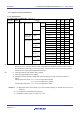
IDD3
Note 5
STOP
mode
T
A = −40°C 0.19 0.50
μ
A
TA = +25°C 0.24 0.50
TA = +50°C 0.32 0.80
TA = +70°C 0.48 1.20
TA = +85°C 0.74 2.20
Notes 1. Total current flowing into VDD, including the input leakage current flowing when the level of the input pin is
fixed to V
DD or VSS. The values below the MAX. column include the peripheral operation current. However,
not including the current flowing into the A/D converter, LVD circuit, I/O port, and on-chip pull-up/pull-down
resistors and the current flowing during data flash rewrite.
2. During HALT instruction execution by flash memory.
3. When high-speed on-chip oscillator clock is stopped.
4. When high-speed system clock is stopped.
5. Not including the current flowing into the 12-bit interval timer and watchdog timer.
6. Relationship between operation voltage width, operation frequency of CPU and operation mode is as
follows.
HS(High speed main) mode: V
DD = 2.7 V to 5.5 V @1 MHz to 24 MHz
VDD = 2.4 V to 5.5 V @1 MHz to 16 MHz
LS(Low speed main) mode: V
DD = 1.8 V to 5.5 V @1 MHz to 8 MHz
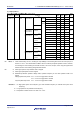
Remarks 1. f
MX: High-speed system clock frequency (X1 clock oscillation frequency or external main system clock
frequency)
2. f
IH: high-speed on-chip oscillator clock frequency
3. Except temperature condition of the TYP. value is TA = 25°C, other than STOP mode
<R>
<R>