Datasheet RL78/G12 R01DS0193EJ0200 Rev.2.00 Sep 06, 2013 RENESAS MCU True Low Power Platform (as low as 63 μA/MHz), 1.8V to 5.5V operation, 2 to 16 Kbyte Flash, 31 DMIPS at 24MHz, for General Purpose Applications 1. OUTLINE 1.1 Features Ultra-Low Power Technology • 1.8 V to 5.5 V operation from a single supply • Stop (RAM retained): 0.23 µA, (LVD enabled): 0.31 µA • Snooze: 0.7 mA (UART), 1.
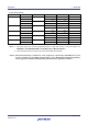
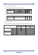
RL78/G12 1. OUTLINE ROM, RAM capacities Code flash Data flash RAM 20 pins 24 pins 30 pins 16 KB 2 KB 2 KB ⎯ ⎯ R5F102AA ⎯ 2 KB ⎯ 1.5 KB ⎯ 12 KB 2KB 1 KB ⎯ 8 KB 2 KB 768 B ⎯ 4 KB 2KB 512 B ⎯ 2 KB 2 KB ⎯ Notes 1.
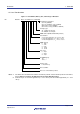
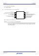
RL78/G12 1. OUTLINE 1.2 List of Part Numbers Figure 1-1. Part Number, Memory Size, and Package of RL78/G12 Part No. R 5 F 1 0 2 A A A x x x S P #V0 Packaging specifications: #U0 : Tray (HWQFN) #V0 : Tray (LSSOP30), Tube (LSSOP20) #W0: Embossed Tape (HWQFN) #X0 : Embossed Tape (LSSOP30, LSSOP20) Package type: SP : LSSOP, 0.65 mm pitch NA : HWQFN, 0.
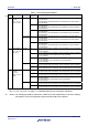
RL78/G12 1. OUTLINE Table 1-1. List of Ordering Part Numbers Pin count 20 pins Package 20-pin plastic LSSOP (4.4 × 6.5 mm, 0.65 mm pitch) Data flash Mounted Not mounted 24 pins 24-pin plastic HWQFN (4 × 4 mm, 0.5 mm pitch) Mounted Not mounted 30 pins 30-pin plastic LSSOP (7.62 mm (300), 0.
RL78/G12 1. OUTLINE 1.3 Differences between the R5F102 Products and the R5F103 Products The following are differences between the R5F102 products and the R5F103 products. Whether the data flash memory is mounted or not High-speed on-chip oscillator oscillation frequency accuracy Number of channels in serial interface Whether the DMA function is mounted or not Whether a part of the safety functions are mounted or not 1.3.
RL78/G12 1. OUTLINE 1.3.2 On-chip oscillator characteristics (1) High-speed on-chip oscillator oscillation frequency of the R5F102 products Oscillator Condition MIN MAX Unit High-speed on-chip oscillator oscillation TA = -20 to +85 °C -1.0 +1.0 % TA = -40 to -20 °C -1.5 +1.5 frequency accuracy TA = +85 to +105 °C -2.0 +2.0 (2) High-speed on-chip oscillator oscillation frequency of the R5F103 products Oscillator Condition MIN MAX Unit High-speed on-chip TA = -40 to + 85 °C -5.0 +5.
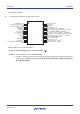
RL78/G12 1. OUTLINE 1.4 Pin Configuration (Top View) 1.4.1 20-pin products • 20-pin plastic LSSOP (4.4 × 6.5 mm, 0.
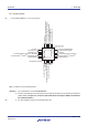
RL78/G12 1. OUTLINE 1.4.2 24-pin products • 24-pin plastic HWQFN (4 × 4 mm, 0.
RL78/G12 1. OUTLINE 1.4.3 30-pin products • 30-pin plastic LSSOP (7.62 mm (300), 0.
RL78/G12 1. OUTLINE 1.
RL78/G12 1. OUTLINE 1.6 Block Diagram 1.6.
RL78/G12 1. OUTLINE 1.6.
RL78/G12 1. OUTLINE 1.6.
RL78/G12 1. OUTLINE 1.7 Outline of Functions This outline describes the function at the time when Peripheral I/O redirection register (PIOR) is set to 00H. (1/2) Item 20-pin R5F1026x Code flash memory Data flash memory RAM 24-pin R5F1036x 2 to 16 KB R5F1027x R5F1037x 2 KB − Note 1 − 512 B to 2KB 1 MB X1, X2 (crystal/ceramic) oscillation, external main system clock input (EXCLK) 1 to 20 MHz: VDD = 2.7 to 5.5 V, 1 to 8 MHz: VDD = 1.8 to 5.5 V system clock R5F103Ax 2 KB 512 B to 1.
RL78/G12 1. OUTLINE (2/2) Item 20-pin R5F1026x 24-pin R5F1036x R5F1027x Clock output/buzzer output 30-pin R5F1037x R5F102Ax 1 R5F103Ax 2 2.
2. ELECTRICAL SPECIFICATIONS (A, D: TA = −40 to +85°C) RL78/G12 2. ELECTRICAL SPECIFICATIONS (A, D: TA = −40 to +85°C) This chapter describes the electrical specifications for the products "A: Consumer applications (TA = -40 to +85°C)" and "D: Industrial applications (TA = -40 to +85°C)". Cautions 1. The RL78 microcontrollers have an on-chip debug function, which is provided for development and evaluation.
2. ELECTRICAL SPECIFICATIONS (A, D: TA = −40 to +85°C) RL78/G12 2.1 Absolute Maximum Ratings Absolute Maximum Ratings (TA = 25°C) Parameter Supply Voltage Symbols Conditions Ratings VDD REGC terminal input Note1 voltage VIREGC REGC Unit −0.5 to + 6.5 V −0.3 to +2.8 V and −0.3 to VDD + 0.3 Note 2 Input Voltage VI1 Other than P60, P61 VI2 P60, P61 (N-ch open drain) Output Voltage VO Analog input voltage VAI −0.3 to VDD + 0.3 IOH1 V Note 3 V −0.3 to 6.5 −0.3 to VDD + 0.
2. ELECTRICAL SPECIFICATIONS (A, D: TA = −40 to +85°C) RL78/G12 2.2 Oscillator Characteristics 2.2.1 X1 oscillator characteristics (TA = −40 to +85°C, 1.8 V ≤ VDD ≤ VDD ≤ 5.5 V, VSS = 0 V) Parameter X1 clock oscillation Note frequency (fX) Note Resonator Ceramic resonator / crystal oscillator Conditions MIN. TYP. MAX. 2.7 V ≤ VDD ≤ 5.5 V 1.0 20.0 1.8 V ≤ VDD < 2.7 V 1.0 8.0 Unit MHz Indicates only permissible oscillator frequency ranges.
2. ELECTRICAL SPECIFICATIONS (A, D: TA = −40 to +85°C) RL78/G12 2.3 DC Characteristics 2.3.1 Pin characteristics (TA = −40 to +85°C, 1.8 V ≤ VDD ≤ 5.5 V, VSS = 0 V) Parameter Symbol Output current, high Note 1 IOH1 (1/4) Conditions MIN. 20-, 24-pin products: Note 4 Per pin for P00 to P03 TYP. MAX. Unit −10.0 mA Note 2 , P10 to P14, P40 to P42 30-pin products: Per pin for P00, P01, P10 to P17, P30, P31, P40, P50, P51, P120, P147 20-, 24-pin products: 4.0 V ≤ VDD ≤ 5.5 V −30.
2. ELECTRICAL SPECIFICATIONS (A, D: TA = −40 to +85°C) RL78/G12 (TA = −40 to +85°C, 1.8 V ≤ VDD ≤ 5.5 V, VSS = 0 V) Parameter Symbol Note 1 Output current, low (2/4) Conditions MIN. 20-, 24-pin products: IOL1 Per pin for P00 to P03 Note 4 TYP. MAX. Unit 20.0 mA Note 2 , P10 to P14, P40 to P42 30-pin products: Per pin for P00, P01, P10 to P17, P30, P31, P40, P50, P51, P120, P147 15.0 Per pin for P60, P61 mA Note 2 20-, 24-pin products: 4.0 V ≤ VDD ≤ 5.5 V 60.
2. ELECTRICAL SPECIFICATIONS (A, D: TA = −40 to +85°C) RL78/G12 (TA = −40 to +85°C, 1.8 V ≤ VDD ≤ 5.5 V, VSS = 0 V) Parameter Input voltage, high Symbol VIH1 (3/4) Conditions MIN. Normal input buffer TYP. MAX. Unit 0.8VDD VDD V Note 2 20-, 24-pin products: P00 to P03 , P10 to P14, P40 to P42 30-pin products: P00, P01, P10 to P17, P30, P31, P40, P50, P51, P120, P147 VIH2 4.0 V ≤ VDD ≤ 5.5 V 2.2 VDD V 20-, 24-pin products: P10, P11 3.3 V ≤ VDD < 4.0 V 2.
2. ELECTRICAL SPECIFICATIONS (A, D: TA = −40 to +85°C) RL78/G12 (TA = −40 to +85°C, 1.8 V ≤ VDD ≤ 5.5 V, VSS = 0 V) Parameter Output voltage, low Symbol VOL1 (4/4) Conditions MAX. Unit 1.3 V 0.7 V 0.6 V 0.4 V 0.4 V IOL2 = 400 μA 0.4 V 4.0 V ≤ VDD ≤ 5.5 V, 2.0 V 0.4 V 0.4 V 0.4 V 1 μA 1 μA 10 μA VI = VSS −1 μA VI = VSS Input port or external clock input −1 μA −10 μA 100 kΩ 20-, 24-pin products: P00 to P03 Note , P10 to P14, IOL1 = 20.0 mA 4.0 V ≤ VDD ≤ 5.
2. ELECTRICAL SPECIFICATIONS (A, D: TA = −40 to +85°C) RL78/G12 2.3.2 Supply current characteristics (1) 20-, 24-pin products (TA = −40 to +85°C, 1.8 V ≤ VDD ≤ 5.5 V, VSS = 0 V) Parameter Supply current Symbol IDD1 Note 1 (1/2) Conditions Note 3 Operating HS(High-speed fIH = 24 MHz Note 4 mode main) mode MIN. Basic 1.5 Normal VDD = 5.0 V operation VDD = 3.0 V 3.3 5.0 3.3 5.0 VDD = 5.0 V 2.5 3.7 VDD = 3.0 V 2.5 3.7 VDD = 3.0 V 1.2 1.8 VDD = 2.0 V 1.2 1.8 Square wave input 2.8 4.
2. ELECTRICAL SPECIFICATIONS (A, D: TA = −40 to +85°C) RL78/G12 (1) 20-, 24-pin products (TA = −40 to +85°C, 1.8 V ≤ VDD ≤ 5.5 V, VSS = 0 V) Parameter Supply current Symbol IDD2 (2/2) Conditions Note 2 Note 1 HALT HS (High-speed mode main) mode fIH = 16 MHz Note 4 fIH = 8 MHz Note 4 Note 6 HS (High-speed main) mode fIH = 24 MHz Note 6 LS (Low-speed main) mode MIN. Note 4 Note 6 fMX = 20 MHz Note 3 , VDD = 5.0 V fMX = 20 MHz Note 3 , VDD = 3.0 V fMX = 10 MHz Note 3 , VDD = 5.
2. ELECTRICAL SPECIFICATIONS (A, D: TA = −40 to +85°C) RL78/G12 (2) 30-pin products (TA = −40 to +85°C, 1.8 V ≤ VDD ≤ 5.5 V, VSS = 0 V) Parameter Supply current Symbol (1/2) Conditions Operating HS (High-speed IDD1 Note 1 mode main) mode MIN. Note 3 Basic fIH = 24 MHz Note 4 VDD = 5.0 V 1.5 operation VDD = 3.0 V 1.5 Normal 3.7 5.5 3.7 5.5 VDD = 5.0 V 2.7 4.0 VDD = 3.0 V 2.7 4.0 VDD = 3.0 V 1.2 1.8 VDD = 2.0 V 1.2 1.8 Square wave input 3.0 4.6 Resonator connection 3.
2. ELECTRICAL SPECIFICATIONS (A, D: TA = −40 to +85°C) RL78/G12 (2) 30-pin products (TA = −40 to +85°C, 1.8 V ≤ VDD ≤ 5.5 V, VSS = 0 V) Parameter Supply current Symbol IDD2 (2/2) Conditions Note 2 Note 1 HALT HS (High-speed mode main) mode fIH = 16 MHz Note 4 fIH = 8 MHz Note 4 Note 6 HS (High-speed main) mode fIH = 24 MHz Note 6 LS (Low-speed main) mode MIN. Note 4 Note 6 fMX = 20 MHz Note 3 , VDD = 5.0 V fMX = 20 MHz Note 3 , VDD = 3.0 V fMX = 10 MHz Note 3 , VDD = 5.
2. ELECTRICAL SPECIFICATIONS (A, D: TA = −40 to +85°C) RL78/G12 (3) Peripheral functions (Common to all products) (TA = −40 to +85°C, 1.8 V ≤ VDD ≤ 5.5 V, VSS = 0 V) Parameter Low-speed Symbol IFIL Conditions MIN. Note 1 TYP. MAX. Unit 0.20 μA 0.02 μA 0.
2. ELECTRICAL SPECIFICATIONS (A, D: TA = −40 to +85°C) RL78/G12 2.4 AC Characteristics (TA = −40 to +85°C, 1.8 V ≤ VDD ≤ 5.5 V, VSS = 0 V) Items Instruction cycle (minimum Symbol TCY instruction execution time) Conditions MIN. TYP. MAX. Unit Main system HS (High- 2.7 V ≤ VDD ≤ 5.5 V 0.04167 1 μs clock (fMAIN) speed main) operation mode 2.4 V ≤ VDD < 2.7 V 0.0625 1 μs 1.8 V ≤ VDD ≤ 5.5 V 0.125 1 μs LS (Lowspeed main) mode During self HS (High- 2.7 V ≤ VDD ≤ 5.5 V 0.
2. ELECTRICAL SPECIFICATIONS (A, D: TA = −40 to +85°C) RL78/G12 Minimum Instruction Execution Time during Main System Clock Operation TCY vs VDD (HS (high-speed main) mode) Cycle time TCY [µs] 10 1.0 When the high-speed on-chip oscillator clock is selected During self programming When high-speed system clock is selected 0.1 0.0625 0.04167 0.01 0 1.0 2.0 3.0 2.4 2.7 4.0 5.0 5.5 6.0 Supply voltage V DD [V] TCY vs VDD (LS (low-speed main) mode) Cycle time TCY [µs] 10 1.
2. ELECTRICAL SPECIFICATIONS (A, D: TA = −40 to +85°C) RL78/G12 AC Timing Test Point VIH/VOH VIH/VOH Test points VIL/VOL VIL/VOL External Main System Clock Timing 1/fEX tEXL tEXH EXCLK TI/TO Timing tTIH tTIL TI00 to TI07 1/fTO TO00 to TO07 Interrupt Request Input Timing tINTH tINTL INTP0 to INTP5 Key Interrupt Input Timing tKR KR0 to KR9 RESET Input Timing tRSL RESET R01DS0193EJ0200 Rev.2.
2. ELECTRICAL SPECIFICATIONS (A, D: TA = −40 to +85°C) RL78/G12 2.5 Peripheral Functions Characteristics AC Timing Test Point VIH/VOH VIH/VOH Test points VIL/VOL VIL/VOL 2.5.1 Serial array unit (1) During communication at same potential (UART mode) (TA = −40 to +85°C, 1.8 V ≤ VDD ≤ 5.5 V, VSS = 0 V) Parameter Symbol Conditions HS (high-speed main) Mode LS (low-speed main) Mode MIN. MIN. Transfer rate Note 1 Theoretical value of the maximum transfer rate fCLK = fMCK Notes 1. 2.
2. ELECTRICAL SPECIFICATIONS (A, D: TA = −40 to +85°C) RL78/G12 (2) During communication at same potential (CSI mode) (master mode, SCK00... internal clock output, corresponding CSI00 only) (TA = −40 to +85°C, 2.7 V ≤ VDD ≤ 5.5 V, VSS = 0 V) Parameter Symbol Conditions HS (high-speed main) LS (low-speed main) Mode Mode MIN. tKCY1 tKCY1 ≥ 2/fCLK SCK00 high-/low- tKH1, level width tKL1 SCK00 cycle time SI00 setup time (to SCK00↑) tSIK1 Note 1 SI00 hold time MIN. MAX. 83.
2. ELECTRICAL SPECIFICATIONS (A, D: TA = −40 to +85°C) RL78/G12 (3) During communication at same potential (CSI mode) (master mode, SCKp... internal clock output) (TA = −40 to +85°C, 1.8 V ≤ VDD ≤ 5.5 V, VSS = 0 V) Parameter Symbol Conditions HS (high-speed LS (low-speed main) main) Mode Mode MIN. SCKp cycle time tKCY1 SCKp high-/low-level width SIp setup time (to SCKp↑) tKCY1 ≥ 4/fCLK 167 500 ns 2.4 V ≤ VDD ≤ 5.5 V 250 500 ns 1.8 V ≤ VDD ≤ 5.5 V − 500 ns 4.0 V ≤ VDD ≤ 5.
2. ELECTRICAL SPECIFICATIONS (A, D: TA = −40 to +85°C) RL78/G12 (4) During communication at same potential (CSI mode) (slave mode, SCKp... external clock input) (TA = −40 to +85°C, 1.8 V ≤ VDD ≤ 5.5 V, VSS = 0 V) Parameter Symbol Conditions HS (high-speed LS (low-speed main) main) Mode Mode MIN. SCKp cycle time Note4 tKCY2 4.0 V ≤ VDD ≤ 5.5 V MAX. MIN. Unit MAX.
2. ELECTRICAL SPECIFICATIONS (A, D: TA = −40 to +85°C) RL78/G12 CSI mode connection diagram (during communication at same potential) SCK SCKp RL78 microcontroller SIp SO User's device SOp SI CSI mode serial transfer timing (during communication at same potential) (When DAPmn = 0 and CKPmn = 0, or DAPmn = 1 and CKPmn = 1.
2. ELECTRICAL SPECIFICATIONS (A, D: TA = −40 to +85°C) RL78/G12 Remarks 1. p: CSI number (p = 00, 01, 11, 20), m: Unit number (m = 0, 1), n: Channel number (n = 0, 1, 3: “1, 3” is only for the R5F102 products.) 2. fMCK: Serial array unit operation clock frequency (Operation clock to be set by the serial clock select register m (SPSm) and the CKSmn bit of serial mode register mn (SMRmn). m: Unit number (m = 0, 1), n: Channel number (n = 0, 1, 3: “1, 3” is only for the R5F102 products.
2. ELECTRICAL SPECIFICATIONS (A, D: TA = −40 to +85°C) RL78/G12 2 Simplified I C mode connection diagram (during communication at same potential) VDD Rb SDA SDAr RL78 microcontroller User's device SCLr SCL 2 Simplified I C mode serial transfer timing (during communication at same potential) 1/fSCL tLOW tHIGH SCLr SDAr tHD:DAT Remarks 1. tSU:DAT Rb [Ω]:Communication line (SDAr) pull-up resistance Cb [F]: Communication line (SCLr, SDAr) load capacitance 2. 3.
2. ELECTRICAL SPECIFICATIONS (A, D: TA = −40 to +85°C) RL78/G12 (6) Communication at different potential (1.8 V, 2.5 V, 3 V) (UART mode) (TA = −40 to +85°C, 1.8 V ≤ VDD ≤ 5.5 V, VSS = 0 V) Parameter Symbol Conditions HS (high-speed main) Mode MIN. Transfer Note4 rate Reception MAX. MIN. Unit MAX. 4.0 V ≤ VDD ≤ 5.5 V, fMCK/6 fMCK/6 2.7 V ≤ Vb ≤ 4.0 V Note1 Note1 4.0 1.3 Mbps 2.7 V ≤ VDD < 4.0 V, fMCK/6 fMCK/6 bps 2.3 V ≤ Vb ≤ 2.7 V Note1 Note1 4.0 1.
2. ELECTRICAL SPECIFICATIONS (A, D: TA = −40 to +85°C) RL78/G12 5. 6. This value as an example is calculated when the conditions described in the “Conditions” column are met. Refer to Note 4 above to calculate the maximum transfer rate under conditions of the customer. The smaller maximum transfer rate derived by using fMCK/6 or the following expression is the valid maximum transfer rate. Expression for calculating the transfer rate when 2.7 V ≤ VDD < 4.0 V and 2.3 V ≤ Vb ≤ 2.
2. ELECTRICAL SPECIFICATIONS (A, D: TA = −40 to +85°C) RL78/G12 UART mode connection diagram (during communication at different potential) Vb Rb Rx TxDq RL78 microcontroller User's device RxDq Tx UART mode bit width (during communication at different potential) (reference) 1/Transfer rate Low-bit width High-bit width Baud rate error tolerance TxDq 1/Transfer rate High-/Low-bit width Baud rate error tolerance RxDq Remarks 1.
2. ELECTRICAL SPECIFICATIONS (A, D: TA = −40 to +85°C) RL78/G12 (7) Communication at different potential (2.5 V, 3 V) (CSI mode) (master mode, SCK00... internal clock output, corresponding CSI00 only) (TA = −40 to +85°C, 2.7 V ≤ VDD ≤ 5.5 V, VSS = 0 V) Parameter Symbol Conditions HS (high-speed LS (low-speed main) Mode main) Mode MIN. SCK00 cycle time tKCY1 tKCY1 ≥ 2/fCLK 4.0 V ≤ VDD ≤ 5.5 V, MAX. MIN. Unit MAX.
2. ELECTRICAL SPECIFICATIONS (A, D: TA = −40 to +85°C) RL78/G12 Notes 1. When DAP00 = 0 and CKP00 = 0, or DAP00 = 1 and CKP00 = 1 2. When DAP00 = 0 and CKP00 = 1, or DAP00 = 1 and CKP00 = 0. Caution Select the TTL input buffer for the SI00 pin and the N-ch open drain output (VDD tolerance) mode for the SO00 pin and SCK00 pin by using port input mode register 1 (PIM1) and port output mode register 1 (POM1). For VIH and VIL, see the DC characteristics with TTL input buffer selected. Remarks 1.
2. ELECTRICAL SPECIFICATIONS (A, D: TA = −40 to +85°C) RL78/G12 (8) Communication at different potential (1.8 V, 2.5 V, 3 V) (CSI mode) (master mode, SCKp... internal clock output) (1/3) (TA = −40 to +85°C, 1.8 V ≤ VDD ≤ VDD ≤ 5.5 V, VSS = 0 V) Parameter Symbol Conditions HS (high-speed main) LS (low-speed main) Mode Mode MIN. SCKp cycle time tKCY1 tKCY1 ≥ 4/fCLK 4.0 V ≤ VDD ≤ 5.5 V, MAX. MIN. Unit MAX.
2. ELECTRICAL SPECIFICATIONS (A, D: TA = −40 to +85°C) RL78/G12 (8) Communication at different potential (1.8 V, 2.5 V, 3 V) (CSI mode) (master mode, SCKp... internal clock output) (2/3) (TA = −40 to +85°C, 1.8 V ≤ VDD ≤ 5.5 V, VSS = 0 V) Parameter Symbol Conditions HS (high-speed LS (low-speed main) Mode main) Mode MIN. SIp setup time (to SCKp↑) tSIK1 Note 1 4.0 V ≤ VDD ≤ 5.5 V, 2.7 V ≤ Vb ≤ 4.0 V, MAX. MIN. Unit MAX.
2. ELECTRICAL SPECIFICATIONS (A, D: TA = −40 to +85°C) RL78/G12 (8) Communication at different potential (1.8 V, 2.5 V, 3 V) (CSI mode) (master mode, SCKp... internal clock output) (3/3) (TA = −40 to +85°C, 1.8 V ≤ VDD ≤ 5.5 V, VSS = 0 V) Parameter Symbol Conditions HS (high-speed LS (low-speed main) Mode main) Mode MIN. SIp setup time (to SCKp↓) 4.0 V ≤ VDD ≤ 5.5 V, 2.7 V ≤ Vb ≤ 4.0 V, tSIK1 Note 1 MAX. MIN. Unit MAX.
2. ELECTRICAL SPECIFICATIONS (A, D: TA = −40 to +85°C) RL78/G12 CSI mode serial transfer timing (master mode) (during communication at different potential) (When DAPmn = 0 and CKPmn = 0, or DAPmn = 1 and CKPmn = 1) t KCY1 t KL1 t KH1 SCKp t SIK1 SIp t KSI1 Input data t KSO1 SOp Output data CSI mode serial transfer timing (master mode) (during communication at different potential) (When DAPmn = 0 and CKPmn = 1, or DAPmn = 1 and CKPmn = 0.
2. ELECTRICAL SPECIFICATIONS (A, D: TA = −40 to +85°C) RL78/G12 (9) Communication at different potential (1.8 V, 2.5 V, 3 V) (CSI mode) (slave mode, SCKp... external clock input) (TA = −40 to +85°C, 1.8 V ≤ VDD ≤ 5.5 V, VSS = 0 V) Parameter Symbol Conditions HS (high-speed main) LS (low-speed main) Mode Mode MIN. SCKp cycle time Note 1 tKCY2 MAX. MIN. Unit MAX. 4.0 V ≤ VDD ≤ 5.5 V, 20 MHz < fMCK ≤ 24 MHz 12/fMCK − ns 2.7 V ≤ Vb ≤ 4.
2. ELECTRICAL SPECIFICATIONS (A, D: TA = −40 to +85°C) RL78/G12 CSI mode connection diagram (during communication at different potential) Vb Rb SCKp RL78 microcontroller SCK SIp SO SOp SI User's device Remarks 1. Rb [Ω]: Communication line (SOp) pull-up resistance, Cb [F]: Communication line (SOp) load capacitance, Vb [V]: Communication line voltage 2. p: CSI number (p = 00, 20), m: Unit number (m = 0, 1), n: Channel number (n = 0) 3.
2. ELECTRICAL SPECIFICATIONS (A, D: TA = −40 to +85°C) RL78/G12 CSI mode serial transfer timing (slave mode) (during communication at different potential) (When DAPmn = 0 and CKPmn = 1, or DAPmn = 1 and CKPmn = 0.) t KCY2 t KL2 t KH2 SCKp t SIK2 SIp t KSI2 Input data t KSO2 SOp Remark Output data p: CSI number (p = 00, 20), m: Unit number (m = 0, 1), n: Channel number (n = 0) R01DS0193EJ0200 Rev.2.
2. ELECTRICAL SPECIFICATIONS (A, D: TA = −40 to +85°C) RL78/G12 2 (10) Communication at different potential (1.8 V, 2.5 V, 3 V) (simplified I C mode) (TA = −40 to +85°C, 1.8 V ≤ VDD ≤ 5.5 V, VSS = 0 V) Parameter Symbol Conditions HS (high-speed LS (low-speed main) Mode main) Mode MIN. SCLr clock frequency fSCL 4.0 V ≤ VDD ≤ 5.5 V, 2.7 V ≤ Vb ≤ 4.0 V, MAX. MIN. Unit MAX. 400 Note1 300 Note1 kHz 400 Note1 300 Note1 kHz 300 Note1 300 Note1 kHz Cb = 100 pF, Rb = 2.8 kΩ 2.
2. ELECTRICAL SPECIFICATIONS (A, D: TA = −40 to +85°C) RL78/G12 2 Simplified I C mode connection diagram (during communication at different potential) Vb Vb Rb Rb SDA SDAr RL78 microcontroller User's device SCLr SCL 2 Simplified I C mode serial transfer timing (during communication at different potential) 1/f SCL t LOW t HIGH SCLr SDAr t HD : DAT Remarks 1.
2. ELECTRICAL SPECIFICATIONS (A, D: TA = −40 to +85°C) RL78/G12 2.5.2 Serial interface IICA (TA = −40 to +85°C, 1.8 V ≤ VDD ≤ 5.5 V, VSS = 0 V) Parameter Symbol Conditions HS (high-speed main) mode Unit LS (low-speed main) mode Standard Mode MIN. MAX. Fast mode: fCLK ≥ 3.5 MHz Fast Mode MIN. MAX. 0 400 SCLA0 clock frequency fSCL Setup time of restart condition tSU:STA 4.7 0.6 μs tHD:STA 4.0 0.6 μs Hold time when SCLA0 = “L” tLOW 4.7 1.3 μs Hold time when SCLA0 = “H” tHIGH 4.
2. ELECTRICAL SPECIFICATIONS (A, D: TA = −40 to +85°C) RL78/G12 2.6 Analog Characteristics 2.6.1 A/D converter characteristics Classification of A/D converter characteristics Input channel Reference Voltage Reference voltage (+) = AVREFP Reference voltage (+) = VDD Reference voltage (+) = VBGR Reference voltage (−) = AVREFM Reference voltage (−) = VSS Reference voltage (−) = AVREFM ANI0 to ANI3 Refer to 2.6.1 (1). Refer to 2.6.1 (3). Refer to 2.6.1 (4). ANI16 to ANI22 Refer to 2.6.1 (2).
2. ELECTRICAL SPECIFICATIONS (A, D: TA = −40 to +85°C) RL78/G12 Notes 1. Excludes quantization error (±1/2 LSB). 2. This value is indicated as a ratio (%FSR) to the full-scale value. 3. When AVREFP < VDD, the MAX. values are as follows. Overall error: Add ±1.0 LSB to the MAX. value when AVREFP = VDD. Zero-scale error/Full-scale error: Add ±0.05%FSR to the MAX. value when AVREFP = VDD. Integral linearity error/ Differential linearity error: Add ±0.5 LSB to the MAX. value when AVREFP = VDD. 4.
2. ELECTRICAL SPECIFICATIONS (A, D: TA = −40 to +85°C) RL78/G12 (3) When reference voltage (+) = VDD (ADREFP1 = 0, ADREFP0 = 0), reference voltage (−) = VSS (ADREFM = 0), target pin: ANI0 to ANI3, ANI16 to ANI22, internal reference voltage, and temperature sensor output voltage (TA = −40 to +85°C, 1.8 V ≤ VDD ≤ 5.5 V, VSS = 0 V, Reference voltage (+) = VDD, Reference voltage (−) = VSS) Parameter Symbol Resolution Conditions RES Note 1 Overall error AINL MIN. TYP. 8 10-bit resolution 1.2 1.
2. ELECTRICAL SPECIFICATIONS (A, D: TA = −40 to +85°C) RL78/G12 (4) When reference voltage (+) = Internal reference voltage (ADREFP1 = 1, ADREFP0 = 0), reference voltage (−) = AVREFM (ADREFM = 1), target pin: ANI0, ANI2, ANI3, and ANI16 to ANI22 (TA = −40 to +85°C, 2.4 V ≤ VDD ≤ 5.5 V, VSS = 0 V, Reference voltage (+) = VBGR Note 3, Reference voltage (−) = AVREFM Note 4 = 0 V, HS (high-speed main) mode) Parameter Symbol Resolution Conditions MIN.
2. ELECTRICAL SPECIFICATIONS (A, D: TA = −40 to +85°C) RL78/G12 2.6.2 Temperature sensor/internal reference voltage characteristics (TA = −40 to +85°C, 2.4 V ≤ VDD ≤ 5.5 V, VSS = 0 V, HS (high-speed main) mode Parameter Symbol Temperature sensor output voltage VTMPS25 Conditions MIN. Setting ADS register = 80H, TYP. MAX. 1.05 Unit V TA = +25°C Internal reference voltage VBGR Setting ADS register = 81H Temperature coefficient FVTMPS Temperature sensor output 1.38 1.45 1.50 V −3.
2. ELECTRICAL SPECIFICATIONS (A, D: TA = −40 to +85°C) RL78/G12 2.6.4 LVD circuit characteristics LVD Detection Voltage of Reset Mode and Interrupt Mode (TA = −40 to +85°C, VPDR ≤ VDD ≤ 5.5 V, VSS = 0 V) Parameter Detection supply voltage Symbol VLVD0 VLVD1 VLVD2 VLVD3 VLVD4 VLVD5 VLVD6 VLVD7 VLVD8 VLVD9 VLVD10 VLVD11 Minimum pulse width Detection delay time R01DS0193EJ0200 Rev.2.00 Sep 06, 2013 tLW Conditions MIN. TYP. MAX. Unit 3.98 4.06 4.14 V Power supply fall time 3.
2. ELECTRICAL SPECIFICATIONS (A, D: TA = −40 to +85°C) RL78/G12 LVD detection voltage of interrupt & reset mode (TA = −40 to +85°C, VPDR ≤ VDD ≤ 5.5 V, VSS = 0 V) Parameter Symbol Interrupt and reset VLVDB0 mode VLVDB1 Conditions LVIS1, LVIS0 = 1, 0 LVIS1, LVIS0 = 0, 1 LVIS1, LVIS0 = 0, 0 VLVDB3 LVIS1, LVIS0 = 1, 0 LVIS1, LVIS0 = 0, 1 VLVDC2 LVIS1, LVIS0 = 0, 0 VLVDC3 Unit 1.80 1.84 1.87 V Rising reset release voltage 1.94 1.98 2.02 V Falling interrupt voltage 1.90 1.
2. ELECTRICAL SPECIFICATIONS (A, D: TA = −40 to +85°C) RL78/G12 2.7 Data Memory STOP Mode Low Supply Voltage Data Retention Characteristics (TA = −40 to +85°C, VSS = 0 V) Parameter Data retention supply voltage Symbol Conditions VDDDR MIN. 1.46 TYP. Note MAX. Unit 5.5 V Note The value depends on the POR detection voltage. When the voltage drops, the data is retained before a POR reset is affected, but data is not retained when a POR reset is affected.
2. ELECTRICAL SPECIFICATIONS (A, D: TA = −40 to +85°C) RL78/G12 2.9 Dedicated Flash Memory Programmer Communication (UART) (TA = −40 to +85°C, 1.8 V ≤ VDD ≤ 5.5 V, VSS = 0 V) Parameter Symbol Transfer rate Conditions MIN. During serial programming TYP. 115,200 MAX. Unit 1,000,000 bps 2.10 Timing of Entry to Flash Memory Programming Modes (TA = −40 to +85°C, 1.8 V ≤ VDD ≤ 5.5 V, VSS = 0 V) Parameter Symbol Time to complete the communication for the initial Conditions MIN. TYP.
3. ELECTRICAL SPECIFICATIONS (G: TA = −40 to +105°C) RL78/G12 3. ELECTRICAL SPECIFICATIONS (G: TA = −40 to +105°C) This chapter describes the electrical specifications for the products "G: Industrial applications (TA = -40 to +105°C)". Cautions 1. The RL78 microcontrollers have an on-chip debug function, which is provided for development and evaluation.
3. ELECTRICAL SPECIFICATIONS (G: TA = −40 to +105°C) RL78/G12 3.1 Absolute Maximum Ratings Absolute Maximum Ratings (TA = 25°C) Parameter Symbols Supply Voltage VDD REGC terminal input Note1 voltage VIREGC Conditions REGC Ratings Unit −0.5 to + 6.5 V −0.3 to +2.8 V and −0.3 to VDD + 0.3 Note 2 Input Voltage VI1 Other than P60, P61 VI2 P60, P61 (N-ch open drain) Output Voltage VO Analog input voltage VAI −0.3 to VDD + 0.3 IOH1 V Note 3 V −0.3 to 6.5 −0.3 to VDD + 0.3 V −0.
3. ELECTRICAL SPECIFICATIONS (G: TA = −40 to +105°C) RL78/G12 3.2 Oscillator Characteristics 3.2.1 X1 oscillator characteristics (TA = −40 to +105°C, 2.4 V ≤ VDD ≤ VDD ≤ 5.5 V, VSS = 0 V) Parameter X1 clock oscillation Note frequency (fX) Resonator Ceramic resonator / crystal oscillator Conditions MIN. TYP. MAX. 2.7 V ≤ VDD ≤ 5.5 V 1.0 20.0 2.4 V ≤ VDD < 2.7 V 1.0 8.0 Unit MHz Note Indicates only permissible oscillator frequency ranges.
3. ELECTRICAL SPECIFICATIONS (G: TA = −40 to +105°C) RL78/G12 3.3 DC Characteristics 3.3.1 Pin characteristics (TA = −40 to +105°C, 2.4 V ≤ VDD ≤ 5.5 V, VSS = 0 V) Parameter Symbol Output current, high Note 1 IOH1 (1/4) Conditions MIN. 20-, 24-pin products: Note 4 Per pin for P00 to P03 TYP. MAX. Unit −3.0 mA Note 2 , P10 to P14, P40 to P42 30-pin products: Per pin for P00, P01, P10 to P17, P30, P31, P40, P50, P51, P120, P147 20-, 24-pin products: 4.0 V ≤ VDD ≤ 5.5 V −9.
3. ELECTRICAL SPECIFICATIONS (G: TA = −40 to +105°C) RL78/G12 (TA = −40 to +105°C, 2.4 V ≤ VDD ≤ 5.5 V, VSS = 0 V) Parameter Symbol Note 1 Output current, low (2/4) Conditions MIN. 20-, 24-pin products: IOL1 Per pin for P00 to P03 Note 4 TYP. MAX. Unit 8.5 mA Note 2 , P10 to P14, P40 to P42 30-pin products: Per pin for P00, P01, P10 to P17, P30, P31, P40, P50, P51, P120, P147 15.0 Per pin for P60, P61 mA Note 2 20-, 24-pin products: 4.0 V ≤ VDD ≤ 5.5 V 25.
3. ELECTRICAL SPECIFICATIONS (G: TA = −40 to +105°C) RL78/G12 (TA = −40 to +105°C, 2.4 V ≤ VDD ≤ 5.5 V, VSS = 0 V) Parameter Input voltage, high Symbol VIH1 (3/4) Conditions MIN. MAX. Unit 0.8VDD VDD V 4.0 V ≤ VDD ≤ 5.5 V 2.2 VDD V 20-, 24-pin products: P10, P11 3.3 V ≤ VDD < 4.0 V 2.0 VDD V 30-pin products: P01, P10, 1.5 VDD V 0.7VDD VDD V 0.7VDD 6.0 V 0.8VDD VDD V 0 0.2VDD V 4.0 V ≤ VDD ≤ 5.5 V 0 0.8 V 20-, 24-pin products: P10, P11 3.3 V ≤ VDD < 4.0 V 0 0.
3. ELECTRICAL SPECIFICATIONS (G: TA = −40 to +105°C) RL78/G12 (TA = −40 to +105°C, 2.4 V ≤ VDD ≤ 5.5 V, VSS = 0 V) Parameter Output voltage, low Symbol VOL1 (4/4) Conditions 20-, 24-pin products: P00 to P03 Note , P10 to P14, MAX. Unit 0.7 V 0.6 V 0.4 V 0.4 V IOL1 = 8.5 mA 2.7 V ≤ VDD ≤ 5.5 V, 30-pin products: P00, P01, IOL1 = 3.0 mA P50, P51, P120, P147 TYP. 4.0 V ≤ VDD ≤ 5.5 V, P40 to P42 P10 to P17, P30, P31, P40, MIN. 2.7 V ≤ VDD ≤ 5.5 V, IOL1 = 1.5 mA 2.4 V ≤ VDD ≤ 5.
3. ELECTRICAL SPECIFICATIONS (G: TA = −40 to +105°C) RL78/G12 3.3.2 Supply current characteristics (1) 20-, 24-pin products (TA = −40 to +105°C, 2.4 V ≤ VDD ≤ 5.5 V, VSS = 0 V) Parameter Supply current Symbol IDD1 Note 1 (1/2) Conditions Operating HS (High-speed mode main) mode MIN. Note 3 Basic fIH = 24 MHz Note 4 VDD = 5.0 V 1.5 operation VDD = 3.0 V 1.5 Normal 3.3 5.3 3.3 5.3 VDD = 5.0 V 2.5 3.9 VDD = 3.0 V 2.5 3.9 Square wave input 2.8 4.7 Resonator connection 3.0 4.
3. ELECTRICAL SPECIFICATIONS (G: TA = −40 to +105°C) RL78/G12 (1) 20-, 24-pin products (TA = −40 to +105°C, 2.4 V ≤ VDD ≤ 5.5 V, VSS = 0 V) Parameter Supply current Symbol IDD2 Note 2 Note 1 (2/2) Conditions HALT mode HS (High-speed main) mode fIH = 24 MHz Note 4 fIH = 16 MHz Note 4 MIN. Note 6 fMX = 20 MHz Note 3 , VDD = 5.0 V fMX = 20 MHz IDD3 Notes 1. VDD = 5.0 V 440 2230 μA VDD = 3.0 V 440 2230 VDD = 5.0 V 400 1650 VDD = 3.
3. ELECTRICAL SPECIFICATIONS (G: TA = −40 to +105°C) RL78/G12 (2) 30-pin products (TA = −40 to +105°C, 2.4 V ≤ VDD ≤ 5.5 V, VSS = 0 V) Parameter Supply current Symbol IDD1 Note 1 (1/2) Conditions Operating HS (High-speed fIH = 24 MHzNote 3 mode main) mode MIN. Basic Note 4 VDD = 5.0 V 1.5 operation VDD = 3.0 V 1.5 Normal MAX. VDD = 5.0 V 3.7 5.8 3.7 5.8 VDD = 5.0 V 2.7 4.2 fIH = 16 MHz VDD = 3.0 V 2.7 4.2 Note 2 Square wave input 3.0 4.9 Resonator connection 3.2 5.
3. ELECTRICAL SPECIFICATIONS (G: TA = −40 to +105°C) RL78/G12 (2) 30-pin products (TA = −40 to +105°C, 2.4 V ≤ VDD ≤ 5.5 V, VSS = 0 V) Parameter Supply current Symbol IDD2 (2/2) Conditions Note 2 Note 1 HALT HS (High-speed mode Note 6 main) mode fIH = 24 MHz Note 4 fIH = 16 MHz Note 4 fMX = 20 MHz MIN. Note 3 , VDD = 5.0 V fMX = 20 MHz IDD3 Notes 1. VDD = 5.0 V 440 2300 μA VDD = 3.0 V 440 2300 VDD = 5.0 V 400 1700 VDD = 3.
3. ELECTRICAL SPECIFICATIONS (G: TA = −40 to +105°C) RL78/G12 (3) Peripheral functions (Common to all products) (TA = −40 to +105°C, 2.4 V ≤ VDD ≤ 5.5 V, VSS = 0 V) Parameter Low-speed onchip Symbol IFIL Conditions MIN. Note 1 TYP. MAX. Unit 0.20 μA 0.02 μA 0.
3. ELECTRICAL SPECIFICATIONS (G: TA = −40 to +105°C) RL78/G12 3.4 AC Characteristics (TA = −40 to +105°C, 2.4 V ≤ VDD ≤ 5.5 V, VSS = 0 V) Items Instruction cycle (minimum Symbol TCY instruction execution time) Conditions fEX frequency External main system clock tEXH, tEXL input high-level width, lowlevel width TI00 to TI07 input high-level 2.7 V ≤ VDD ≤ 5.5 V 0.04167 1 μs speed main) operation mode 2.4 V ≤ VDD < 2.7 V 0.0625 1 μs During self HS (High- 2.7 V ≤ VDD ≤ 5.5 V 0.
3. ELECTRICAL SPECIFICATIONS (G: TA = −40 to +105°C) RL78/G12 Minimum Instruction Execution Time during Main System Clock Operation TCY vs VDD (HS (high-speed main) mode) Cycle time TCY [µs] 10 1.0 When the high-speed on-chip oscillator clock is selected During self programming When high-speed system clock is selected 0.1 0.0625 0.04167 0.01 0 1.0 2.0 3.0 2.4 2.7 4.0 5.0 5.5 6.
3. ELECTRICAL SPECIFICATIONS (G: TA = −40 to +105°C) RL78/G12 TI/TO Timing tTIH tTIL TI00 to TI07 1/fTO TO00 to TO07 Interrupt Request Input Timing tINTH tINTL INTP0 to INTP5 Key Interrupt Input Timing tKR KR0 to KR9 RESET Input Timing tRSL RESET R01DS0193EJ0200 Rev.2.
3. ELECTRICAL SPECIFICATIONS (G: TA = −40 to +105°C) RL78/G12 3.5 Peripheral Functions Characteristics AC Timing Test Point VIH/VOH VIH/VOH Test points VIL/VOL VIL/VOL 3.5.1 Serial array unit (1) During communication at same potential (UART mode) (TA = −40 to +105°C, 2.4 V ≤ VDD ≤ 5.5 V, VSS = 0 V) Parameter Symbol Conditions HS (high-speed main) Mode MIN. Transfer rate Note 1 MAX. fMCK/12 bps 2.0 Mbps Theoretical value of the maximum transfer rate fCLK = fMCK Notes 1. 2.
3. ELECTRICAL SPECIFICATIONS (G: TA = −40 to +105°C) RL78/G12 (2) During communication at same potential (CSI mode) (master mode, SCKp... internal clock output) (TA = −40 to +105°C, 2.4 V ≤ VDD ≤ 5.5 V, VSS = 0 V) Parameter Symbol Conditions HS (high-speed main) Mode MIN. SCKp cycle time tKCY1 SCKp high-/low-level width SIp setup time (to SCKp↑) Note 1 SIp hold time (from SCKp↑) Note 2 Delay time from SCKp↓ to SOp output tKCY1 ≥ 4/fCLK Unit MAX. 2.7 V ≤ VDD ≤ 5.5 V 334 ns 2.
3. ELECTRICAL SPECIFICATIONS (G: TA = −40 to +105°C) RL78/G12 (3) During communication at same potential (CSI mode) (slave mode, SCKp... external clock input) (TA = −40 to +105°C, 2.4 V ≤ VDD ≤ 5.5 V, VSS = 0 V) Parameter Symbol Conditions HS (high-speed main) Mode MIN. SCKp cycle time Note4 tKCY2 4.0 V ≤ VDD ≤ 5.5 V 2.7 V ≤ VDD ≤ 5.5 V Unit MAX. 20 MHz < fMCK 16/fMCK ns fMCK ≤ 20 MHz 12/fMCK ns 16 MHz < fMCK 16/fMCK ns fMCK ≤ 16 MHz 12/fMCK ns 12/fMCK ns 2.4 V ≤ VDD ≤ 5.
3. ELECTRICAL SPECIFICATIONS (G: TA = −40 to +105°C) RL78/G12 CSI mode serial transfer timing (during communication at same potential) (When DAPmn = 0 and CKPmn = 0, or DAPmn = 1 and CKPmn = 1.) tKCY1, 2 tKL1, 2 tKH1, 2 SCKp tSIK1, 2 SIp tKSI1, 2 Input data tKSO1, 2 SOp Output data CSI mode serial transfer timing (during communication at same potential) (When DAPmn = 0 and CKPmn = 1, or DAPmn = 1 and CKPmn = 0.
3. ELECTRICAL SPECIFICATIONS (G: TA = −40 to +105°C) RL78/G12 2 (4) During communication at same potential (simplified I C mode) (TA = −40 to +105°C, 2.4 V ≤ VDD ≤ 5.5 V, VSS = 0 V) Parameter Symbol Conditions HS (high-speed main) Mode MIN.
3. ELECTRICAL SPECIFICATIONS (G: TA = −40 to +105°C) RL78/G12 (5) Communication at different potential (1.8 V, 2.5 V, 3 V) (UART mode) (TA = −40 to +105°C, 2.4 V ≤ VDD ≤ 5.5 V, VSS = 0 V) Parameter Symbol HS (high-speed main) Conditions Unit Mode MIN. Reception Transfer rate MAX. 4.0 V ≤ VDD ≤ 5.5 V, fMCK/12 Theoretical value of the maximum transfer rate Note 2 fMCK = fCLK 2.7 V ≤ VDD < 4.0 V, 2.0 Mbps fMCK/12 bps Note 1 2.3 V ≤ Vb ≤ 2.7 V 2.0 Mbps 2.4 V ≤ VDD < 3.
3. ELECTRICAL SPECIFICATIONS (G: TA = −40 to +105°C) RL78/G12 4. This value as an example is calculated when the conditions described in the “Conditions” column are met. Refer to Note 3 above to calculate the maximum transfer rate under conditions of the customer. 5. The smaller maximum transfer rate derived by using fMCK/12 or the following expression is the valid maximum transfer rate. Expression for calculating the transfer rate when 2.7 V ≤ VDD < 4.0 V and 2.3 V ≤ Vb ≤ 2.
3. ELECTRICAL SPECIFICATIONS (G: TA = −40 to +105°C) RL78/G12 UART mode connection diagram (during communication at different potential) Vb Rb Rx TxDq RL78 microcontroller User's device RxDq Tx UART mode bit width (during communication at different potential) (reference) 1/Transfer rate Low-bit width High-bit width Baud rate error tolerance TxDq 1/Transfer rate High-/Low-bit width Baud rate error tolerance RxDq Remarks 1.
3. ELECTRICAL SPECIFICATIONS (G: TA = −40 to +105°C) RL78/G12 (6) Communication at different potential (1.8 V, 2.5 V, 3 V) (CSI mode) (master mode, SCKp... internal clock output) (1/3) (TA = −40 to +105°C, 2.4 V ≤ VDD ≤ VDD ≤ 5.5 V, VSS = 0 V) Parameter Symbol Conditions HS (high-speed main) Mode MIN. SCKp cycle time tKCY1 tKCY1 ≥ 4/fCLK 4.0 V ≤ VDD ≤ 5.5 V, Unit MAX.
3. ELECTRICAL SPECIFICATIONS (G: TA = −40 to +105°C) RL78/G12 (6) Communication at different potential (1.8 V, 2.5 V, 3 V) (CSI mode) (master mode, SCKp... internal clock output) (2/3) (TA = −40 to +105°C, 2.4 V ≤ VDD ≤ 5.5 V, VSS = 0 V) Parameter Symbol Conditions HS (high-speed main) Mode MIN. SIp setup time (to SCKp↑) tSIK1 Note 4.0 V ≤ VDD ≤ 5.5 V, 2.7 V ≤ Vb ≤ 4.0 V, Unit MAX. 162 ns 354 ns 958 ns 38 ns 38 ns 38 ns Cb = 30 pF, Rb = 1.4 kΩ 2.7 V ≤ VDD < 4.0 V, 2.3 V ≤ Vb ≤ 2.
3. ELECTRICAL SPECIFICATIONS (G: TA = −40 to +105°C) RL78/G12 (6) Communication at different potential (1.8 V, 2.5 V, 3 V) (CSI mode) (master mode, SCKp... internal clock output) (3/3) (TA = −40 to +105°C, 2.4 V ≤ VDD ≤ 5.5 V, VSS = 0 V) Parameter Symbol Conditions HS (high-speed main) Mode MIN. SIp setup time (to SCKp↓) 4.0 V ≤ VDD ≤ 5.5 V, 2.7 V ≤ Vb ≤ 4.0 V, tSIK1 Note Unit MAX. 88 ns 88 ns 220 ns 38 ns 38 ns 38 ns Cb = 30 pF, Rb = 1.4 kΩ 2.7 V ≤ VDD < 4.0 V, 2.3 V ≤ Vb ≤ 2.
3. ELECTRICAL SPECIFICATIONS (G: TA = −40 to +105°C) RL78/G12 CSI mode serial transfer timing (master mode) (during communication at different potential) (When DAPmn = 0 and CKPmn = 0, or DAPmn = 1 and CKPmn = 1) t KCY1 t KL1 t KH1 SCKp t SIK1 SIp t KSI1 Input data t KSO1 SOp Output data CSI mode serial transfer timing (master mode) (during communication at different potential) (When DAPmn = 0 and CKPmn = 1, or DAPmn = 1 and CKPmn = 0.
3. ELECTRICAL SPECIFICATIONS (G: TA = −40 to +105°C) RL78/G12 (7) Communication at different potential (1.8 V, 2.5 V, 3 V) (CSI mode) (slave mode, SCKp... external clock input) (TA = −40 to +105°C, 2.4 V ≤ VDD ≤ 5.5 V, VSS = 0 V) Parameter Symbol HS (high-speed main) Conditions Unit Mode MIN. SCKp cycle time Note 1 tKCY2 MAX. 4.0 V ≤ VDD ≤ 5.5 V, 20 MHz < fMCK ≤ 24 MHz 24/fMCK ns 2.7 V ≤ Vb ≤ 4.
3. ELECTRICAL SPECIFICATIONS (G: TA = −40 to +105°C) RL78/G12 CSI mode connection diagram (during communication at different potential) Vb Rb SCKp RL78 microcontroller SCK SIp SO SOp SI User's device CSI mode serial transfer timing (slave mode) (during communication at different potential) (When DAPmn = 0 and CKPmn = 0, or DAPmn = 1 and CKPmn = 1.) t KCY2 t KH2 t KL2 SCKp t SIK2 t KSI2 Input data SIp t KSO2 SOp Output data Remarks 1.
3. ELECTRICAL SPECIFICATIONS (G: TA = −40 to +105°C) RL78/G12 CSI mode serial transfer timing (slave mode) (during communication at different potential) (When DAPmn = 0 and CKPmn = 1, or DAPmn = 1 and CKPmn = 0.) t KCY2 t KL2 t KH2 SCKp t SIK2 SIp t KSI2 Input data t KSO2 SOp Remark Output data p: CSI number (p = 00, 20), m: Unit number (m = 0, 1), n: Channel number (n = 0) R01DS0193EJ0200 Rev.2.
3. ELECTRICAL SPECIFICATIONS (G: TA = −40 to +105°C) RL78/G12 2 (8) Communication at different potential (1.8 V, 2.5 V, 3 V) (simplified I C mode) (TA = −40 to +105°C, 2.4 V ≤ VDD ≤ 5.5 V, VSS = 0 V) Parameter Symbol Conditions HS (high-speed main) Unit Mode MIN. SCLr clock frequency fSCL 4.0 V ≤ VDD ≤ 5.5 V, 2.7 V ≤ Vb ≤ 4.0 V, MAX. 100 Note1 kHz 100 Note1 kHz 100 Note1 kHz Cb = 100 pF, Rb = 2.8 kΩ 2.7 V ≤ VDD < 4.0 V, 2.3 V ≤ Vb ≤ 2.7 V, Cb = 100 pF, Rb = 2.7 kΩ 2.4 V ≤ VDD < 3.
3. ELECTRICAL SPECIFICATIONS (G: TA = −40 to +105°C) RL78/G12 2 Simplified I C mode connection diagram (during communication at different potential) Vb Vb Rb Rb SDA SDAr RL78 microcontroller User's device SCLr SCL 2 Simplified I C mode serial transfer timing (during communication at different potential) 1/f SCL t LOW t HIGH SCLr SDAr t HD : DAT Remarks 1.
3. ELECTRICAL SPECIFICATIONS (G: TA = −40 to +105°C) RL78/G12 3.5.2 Serial interface IICA (TA = −40 to +105°C, 2.4 V ≤ VDD ≤ 5.5 V, VSS = 0 V) Parameter Symbol Conditions HS (high-speed main) mode Standard Mode MIN. SCLA0 clock frequency fSCL Fast mode: fCLK ≥ 3.5 MHz Normal mode: fCLK ≥ 1 MHz Setup time of restart condition MAX. 0 Unit Fast Mode MIN. MAX. 0 400 100 kHz kHz tSU:STA 4.7 0.6 μs tHD:STA 4.0 0.6 μs Hold time when SCLA0 = “L” tLOW 4.7 1.
3. ELECTRICAL SPECIFICATIONS (G: TA = −40 to +105°C) RL78/G12 3.6 Analog Characteristics 3.6.1 A/D converter characteristics Classification of A/D converter characteristics Input channel Reference Voltage Reference voltage (+) = AVREFP Reference voltage (+) = VDD Reference voltage (+) = VBGR Reference voltage (−) = AVREFM Reference voltage (−) = VSS Reference voltage (−) = AVREFM ANI0 to ANI3 Refer to 3.6.1 (1). Refer to 3.6.1 (3). Refer to 3.6.1 (4). ANI16 to ANI22 Refer to 3.6.1 (2).
3. ELECTRICAL SPECIFICATIONS (G: TA = −40 to +105°C) RL78/G12 Notes 1. Excludes quantization error (±1/2 LSB). 2. This value is indicated as a ratio (%FSR) to the full-scale value. 3. When AVREFP < VDD, the MAX. values are as follows. Overall error: Add ±1.0 LSB to the MAX. value when AVREFP = VDD. Zero-scale error/Full-scale error: Add ±0.05%FSR to the MAX. value when AVREFP = VDD. Integral linearity error/ Differential linearity error: Add ±0.5 LSB to the MAX. value when AVREFP = VDD. 4. Refer to 3.6.
3. ELECTRICAL SPECIFICATIONS (G: TA = −40 to +105°C) RL78/G12 (3) When reference voltage (+) = VDD (ADREFP1 = 0, ADREFP0 = 0), reference voltage (−) = VSS (ADREFM = 0), target pin: ANI0 to ANI3, ANI16 to ANI22, internal reference voltage, and temperature sensor output voltage (TA = −40 to +105°C, 2.4 V ≤ VDD ≤ 5.5 V, VSS = 0 V, Reference voltage (+) = VDD, Reference voltage (−) = VSS) Parameter Symbol Resolution Conditions RES Note 1 MIN. TYP. 8 Unit 10 bit ±7.
3. ELECTRICAL SPECIFICATIONS (G: TA = −40 to +105°C) RL78/G12 (4) When reference voltage (+) = Internal reference voltage (ADREFP1 = 1, ADREFP0 = 0), reference voltage (−) = AVREFM (ADREFM = 1), target pin: ANI0, ANI2, ANI3, and ANI16 to ANI22 (TA = −40 to +105°C, 2.4 V ≤ VDD ≤ 5.5 V, VSS = 0 V, Reference voltage (+) = VBGR Note 3, Reference voltage (−) = AVREFM Note 4= 0 V, HS (high-speed main) mode) Parameter Symbol Resolution Conditions MIN.
3. ELECTRICAL SPECIFICATIONS (G: TA = −40 to +105°C) RL78/G12 3.6.2 Temperature sensor/internal reference voltage characteristics (TA = −40 to +105°C, 2.4 V ≤ VDD ≤ 5.5 V, VSS = 0 V, HS (high-speed main) mode Parameter Symbol Temperature sensor output voltage VTMPS25 Conditions MIN. Setting ADS register = 80H, TYP. MAX. 1.05 Unit V TA = +25°C Internal reference voltage VBGR Setting ADS register = 81H Temperature coefficient FVTMPS Temperature sensor output 1.38 1.45 1.50 −3.
3. ELECTRICAL SPECIFICATIONS (G: TA = −40 to +105°C) RL78/G12 3.6.4 LVD circuit characteristics LVD Detection Voltage of Reset Mode and Interrupt Mode (TA = −40 to +105°C, VPDR ≤ VDD ≤ 5.5 V, VSS = 0 V) Parameter Detection supply voltage Symbol MAX. Unit 3.90 4.06 4.22 V Power supply fall time 3.83 3.98 4.13 V VLVD1 Power supply rise time 3.60 3.75 3.90 V Power supply fall time 3.53 3.67 3.81 V Power supply rise time 3.01 3.13 3.25 V Power supply fall time 2.94 3.06 3.
3. ELECTRICAL SPECIFICATIONS (G: TA = −40 to +105°C) RL78/G12 LVD detection voltage of interrupt & reset mode (TA = −40 to +105°C, VPDR ≤ VDD ≤ 5.5 V, VSS = 0 V) Parameter Symbol Interrupt and reset VLVDD0 mode VLVDD1 Conditions MIN. TYP. MAX. Unit 2.64 2.75 2.86 V Rising reset release voltage 2.81 2.92 3.03 V Falling interrupt voltage 2.75 2.86 2.97 V Rising reset release voltage 2.90 3.02 3.14 V Falling interrupt voltage 2.85 2.96 3.
3. ELECTRICAL SPECIFICATIONS (G: TA = −40 to +105°C) RL78/G12 3.7 Data Memory STOP Mode Low Supply Voltage Data Retention Characteristics (TA = −40 to +105°C, VSS = 0 V) Parameter Data retention supply voltage Symbol Conditions VDDDR MIN. 1.44 TYP. MAX. Unit 5.5 V Note Note The value depends on the POR detection voltage. When the voltage drops, the data is retained before a POR reset is affected, but data is not retained when a POR reset is affected.
3. ELECTRICAL SPECIFICATIONS (G: TA = −40 to +105°C) RL78/G12 3.9 Dedicated Flash Memory Programmer Communication (UART) (TA = −40 to +105°C, 2.4 V ≤ VDD ≤ 5.5 V, VSS = 0 V) Parameter Symbol Transfer rate Conditions MIN. During serial programming TYP. 115,200 MAX. Unit 1,000,000 bps 3.10 Timing of Entry to Flash Memory Programming Modes (TA = −40 to +105°C, 2.4 V ≤ VDD ≤ 5.5 V, VSS = 0 V) Parameter Symbol Time to complete the communication for the initial tSUINIT Conditions MIN.
RL78/G12 4. PACKAGE DRAWINGS 4. PACKAGE DRAWINGS 4.
RL78/G12 4. PACKAGE DRAWINGS 4.2 24-pin products R5F1027AANA, R5F10279ANA, R5F10278ANA, R5F10277ANA R5F1037AANA, R5F10379ANA, R5F10378ANA, R5F10377ANA R5F1027ADNA, R5F10279DNA, R5F10278DNA, R5F10277DNA R5F1037ADNA, R5F10379DNA, R5F10378DNA, R5F10377DNA R5F1027AGNA, R5F10279GNA, R5F10278GNA, R5F10277GNA R5F1037AGNA, R5F10379GNA, R5F10378GNA, R5F10377GNA JEITA Package Code RENESAS Code Previous Code MASS (TYP.) [g] P-HWQFN24-4x4-0.50 PWQN0024KE-A P24K8-50-CAB-1 0.
RL78/G12 4. PACKAGE DRAWINGS 4.3 30-pin products R5F102AAASP, R5F102A9ASP, R5F102A8ASP, R5F102A7ASP R5F103AAASP, R5F103A9ASP, R5F103A8ASP, R5F103A7ASP R5F102AADSP, R5F102A9DSP, R5F102A8DSP, R5F102A7DSP R5F103AADSP, R5F103A9DSP, R5F103A8DSP, R5F103A7DSP R5F102AAGSP, R5F102A9GSP, R5F102A8GSP, R5F102A7GSP R5F103AAGSP, R5F103A9GSP, R5F103A8GSP, R5F103A7GSP JEITA Package Code RENESAS Code Previous Code MASS (TYP.) [g] P-LSSOP30-0300-0.65 PLSP0030JB-B S30MC-65-5A4-3 0.
Revision History RL78/G12 Data Sheet Description Rev. Date Page 1.00 Dec 10, 2012 - First Edition issued 2.00 Sep 06, 2013 1 Modification of 1.1 Features 3 Modification of 1.2 List of Part Numbers 4 Modification of Table 1-1. List of Ordering Part Numbers, Note, and Caution 7 to 9 Summary Modification of package name in 1.4.1 to 1.4.3 14 Modification of tables in 1.7 Outline of Functions 17 Modification of description of table in 2.
Description Rev. Date Page 2.00 Sep 06, 2013 55 Modification of description and Notes 3 and 4 in 2.6.1 (3) 56 Modification of description and Notes 3 and 4 in 2.6.1 (4) 57 Modification of table in 2.6.2 Temperature sensor/internal reference voltage characteristics 57 Modification of table and Note in 2.6.3 POR circuit characteristics 58 Modification of table in 2.6.
NOTES FOR CMOS DEVICES (1) VOLTAGE APPLICATION WAVEFORM AT INPUT PIN: Waveform distortion due to input noise or a reflected wave may cause malfunction. If the input of the CMOS device stays in the area between VIL (MAX) and VIH (MIN) due to noise, etc., the device may malfunction. Take care to prevent chattering noise from entering the device when the input level is fixed, and also in the transition period when the input level passes through the area between VIL (MAX) and VIH (MIN).
Notice 1. Descriptions of circuits, software and other related information in this document are provided only to illustrate the operation of semiconductor products and application examples. You are fully responsible for the incorporation of these circuits, software, and information in the design of your equipment. Renesas Electronics assumes no responsibility for any losses incurred by you or third parties arising from the use of these circuits, software, or information. 2.