
Datasheet

RL78/G12 2. ELECTRICAL SPECIFICATIONS (A, D: T
A = −40 to +85°C)
R01DS0193EJ0200 Rev.2.00
Sep 06, 2013
Page 47 of 106
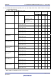
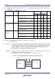
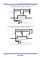
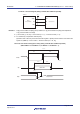
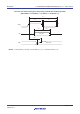
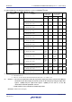
(9) Communication at different potential (1.8 V, 2.5 V, 3 V) (CSI mode) (slave mode, SCKp... external clock input)
(TA = −40 to +85°C, 1.8 V ≤ VDD ≤ 5.5 V, VSS = 0 V)
Parameter Symbol Conditions
HS (high-speed main)
Mode
LS (low-speed main)
Mode
Unit
MIN. MAX. MIN. MAX.
SCKp cycle time
Note 1
tKCY2 4.0 V ≤ VDD ≤ 5.5 V,
2.7 V ≤ V
b ≤ 4.0 V
20 MHz < f
MCK ≤ 24 MHz 12/fMCK
−
ns
8 MHz < fMCK ≤ 20 MHz 10/fMCK
−
ns
4 MHz < fMCK ≤ 8 MHz 8/fMCK 16/fMCK ns
fMCK ≤ 4 MHz 6/fMCK 10/fMCK ns
2.7 V ≤ VDD < 4.0 V,
2.3 V ≤ V
b ≤ 2.7 V
20 MHz < f
MCK ≤ 24 MHz 16/fMCK
−
ns
16 MHz < fMCK ≤ 20 MHz 14/fMCK
−
ns
8 MHz < fMCK ≤ 16 MHz 12/fMCK
−
ns
4 MHz < fMCK ≤ 8 MHz 8/fMCK 16/fMCK ns
fMCK ≤ 4 MHz
6/fMCK 10/fMCK ns
1.8 V ≤ VDD < 3.3 V,
1.6 V ≤ V
b ≤ 2.0 V
Note 2
20 MHz < f
MCK ≤ 24 MHz 36/fMCK
−
ns
16 MHz < fMCK ≤ 20 MHz 32/fMCK
−
ns
8 MHz < fMCK ≤ 16 MHz 26/fMCK
−
ns
4 MHz < fMCK ≤ 8 MHz
16/fMCK 16/fMCK ns
fMCK ≤ 4 MHz
10/fMCK 10/fMCK ns
SCKp high-/low-level
width
tKH2,
t
KL2
4.0 V ≤ V
DD ≤ 5.5 V, 2.7 V ≤ Vb ≤ 4.0 V
t
KCY2/2 − 12 tKCY2/2 − 50 ns
2.7 V ≤ VDD < 4.0 V, 2.3 V ≤ Vb ≤ 2.7 V
t
KCY2/2 − 18 tKCY2/2 − 50 ns
1.8 V ≤ VDD < 3.3 V, 1.6 V ≤ Vb ≤ 2.0 V
Note 2
t
KCY2/2 − 50 tKCY2/2 − 50 ns
SIp setup time
(to SCKp↑)
Note 3
t
SIK2 4.0 V ≤ VDD ≤ 5.5 V, 2.7 V ≤ VDD ≤ 4.0 V
1/f
MCK
+
20
1/fMCK
+
30 ns
2.7 V ≤ VDD < 4.0 V, 2.3 V ≤ Vb ≤ 2.7 V
1/f
MCK
+
20
1/fMCK
+
30 ns
1.8 V ≤ VDD < 3.3 V, 1.6 V ≤ VDD ≤ 2.0 V
Note 2
1/f
MCK
+ 30
1/fMCK
+
30 ns
SIp hold time
(from SCKp↑)
Note 4
t
KSI2
1/f
MCK
+ 31
1/fMCK
+
31 ns
Delay time from
SCKp↓ to SOp
output
Note 5
t
KSO2 4.0 V ≤ VDD ≤ 5.5 V, 2.7 V ≤ Vb ≤ 4.0 V,
C
b = 30 pF, Rb = 1.4 kΩ
2/f
MCK +
120
2/fMCK
+
573
ns
2.7 V ≤ VDD < 4.0 V, 2.3 V ≤ Vb ≤ 2.7 V,
C
b = 30 pF, Rb = 2.7 kΩ
2/f
MCK +
214
2/f
MCK
+
573
ns
1.8 V ≤ VDD < 3.3 V, 1.6 V ≤ Vb ≤ 2.0 V
Note 2
,
C
b = 30 pF, Rb = 5.5 kΩ
2/f
MCK +
573
2/f
MCK
+
573
ns
Notes 1. Transfer rate in the SNOOZE mode: MAX. 1 Mbps
2. Use it with V
DD ≥ Vb.
3. When DAPmn = 0 and CKPmn = 0, or DAPmn = 1 and CKPmn = 1. The SIp setup time becomes “to
SCKp↓” when DAPmn = 0 and CKPmn = 1, or DAPmn = 1 and CKPmn = 0.
4. When DAPmn = 0 and CKPmn = 0, or DAPmn = 1 and CKPmn = 1. The SIp hold time becomes “from
SCKp↓” when DAPmn = 0 and CKPmn = 1, or DAPmn = 1 and CKPmn = 0.
5. When DAPmn = 0 and CKPmn = 0, or DAPmn = 1 and CKPmn = 1. The delay time to SOp output
becomes “from SCKp↑” when DAPmn = 0 and CKPmn = 1, or DAPmn = 1 and CKPmn = 0.
Cautions 1. Select the TTL input buffer for the SIp and SCKp pins and the N-ch open drain output (V
DD
tolerance) mode for the SOp pin by using port input mode register 1 (PIM1) and port output mode
register 1 (POM1). For V
IH and VIL, see the DC characteristics with TTL input buffer selected.
2. CSI01 and CSI11 cannot communicate at different potential.
<R>