
Datasheet


RL78/G12 2. ELECTRICAL SPECIFICATIONS (A, D: T
A = −40 to +85°C)
R01DS0193EJ0200 Rev.2.00
Sep 06, 2013
Page 33 of 106
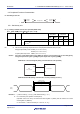
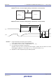
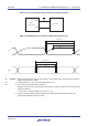
(3) During communication at same potential (CSI mode) (master mode, SCKp... internal clock output)
(TA = −40 to +85°C, 1.8 V ≤ VDD ≤ 5.5 V, VSS = 0 V)
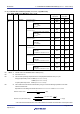
Parameter Symbol Conditions
HS (high-speed
main) Mode
LS (low-speed main)
Mode
Unit
MIN. MAX. MIN. MAX.
SCKp cycle time tKCY1 tKCY1 ≥ 4/fCLK 2.7 V ≤ VDD ≤ 5.5 V 167 500 ns
2.4 V ≤ VDD ≤ 5.5 V 250 500 ns
1.8 V ≤ VDD ≤ 5.5 V
−
500 ns
SCKp high-/low-level width tKH1,
t
KL1
4.0 V ≤ V
DD ≤ 5.5 V tKCY1/2−12 tKCY1/2−50 ns
2.7 V ≤ VDD ≤ 5.5 V tKCY1/2−18 tKCY1/2−50 ns
2.4 V ≤ VDD ≤ 5.5 V tKCY1/2−38 tKCY1/2−50 ns
1.8 V ≤ VDD ≤ 5.5 V
−
tKCY1/2−50 ns
SIp setup time (to SCKp↑)
Note 1
t
SIK1 4.0 V ≤ VDD ≤ 5.5 V 44 110 ns
2.7 V ≤ VDD ≤ 5.5 V 44 110 ns
2.4 V ≤ VDD ≤ 5.5 V 75 110 ns
1.8 V ≤ VDD ≤ 5.5 V
−
110 ns
SIp hold time
(from SCKp↑)
Note 2
t
KSI1 19 19 ns
Delay time from SCKp↓ to
SOp output
Note 3
t
KSO1 C = 30 pF
Note4
25 25 ns
Notes 1. When DAPmn = 0 and CKPmn = 0, or DAPmn = 1 and CKPmn = 1. The SIp setup time becomes “to
SCKp↓” when DAPmn = 0 and CKPmn = 1, or DAPmn = 1 and CKPmn = 0.
2. When DAPmn = 0 and CKPmn = 0, or DAPmn = 1 and CKPmn = 1. The SIp hold time becomes “from
SCKp↓” when DAPmn = 0 and CKPmn = 1, or DAPmn = 1 and CKPmn = 0.
3. When DAPmn = 0 and CKPmn = 0, or DAPmn = 1 and CKPmn = 1. The delay time to SOp output
becomes “from SCKp↑” when DAPmn = 0 and CKPmn = 1, or DAPmn = 1 and CKPmn = 0.
4. C is the load capacitance of the SCKp and SOp output lines.
Caution Select the normal input buffer for the SIp pin and the normal output mode for the SOp and SCKp pins
by using port input mode register 1 (PIM1) and port output mode registers 0, 1, 4 (POM0, POM1,
POM4).
Remarks 1. p: CSI number (p = 00, 01, 11, 20), m: Unit number (m = 0, 1), n: Channel number (n = 0, 1, 3: “1, 3” is
only for the R5F102 products)
2. f
MCK: Serial array unit operation clock frequency
(Operation clock to be set by the serial clock select register m (SPSm) and the CKSmn bit of serial mode
register mn (SMRmn). m: Unit number (m = 0, 1), n: Channel number (n = 0, 1, 3: “1, 3” is only for the
R5F102 products.))
<R>