
Datasheet


RL78/G12 2. ELECTRICAL SPECIFICATIONS (A, D: T
A = −40 to +85°C)
R01DS0193EJ0200 Rev.2.00
Sep 06, 2013
Page 28 of 106
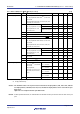
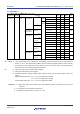
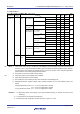
2.4 AC Characteristics
(TA = −40 to +85°C, 1.8 V ≤ VDD ≤ 5.5 V, VSS = 0 V)
Items Symbol Conditions MIN. TYP. MAX. Unit
Instruction cycle (minimum
instruction execution time)
T
CY
Main system
clock (f
MAIN
)
operation
HS (High-
speed main)
mode
2.7 V ≤ VDD ≤ 5.5 V 0.04167 1
μ
s
2.4 V ≤ VDD < 2.7 V 0.0625 1
μ
s
LS (Low-
speed main)
mode
1.8 V ≤ V
DD ≤ 5.5 V 0.125 1
μ
s
During self
programming
HS (High-
speed main)
mode
2.7 V ≤ VDD ≤ 5.5 V 0.04167 1
μ
s
2.4 V ≤ VDD < 2.7 V 0.0625 1
μ
s
LS (Low-
speed main)
mode
1.8 V ≤ V
DD ≤ 5.5 V 0.125 1
μ
s
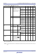
External main system clock
frequency
f
EX 2.7 V ≤ VDD ≤ 5.5 V 1.0 20.0 MHz
2.4 V ≤ VDD < 2.7 V 1.0 16.0 MHz
1.8 V ≤ VDD < 2.4 V 1.0 8.0 MHz
External main system clock
input high-level width, low-
level width
t
EXH, tEXL 2.7 V ≤ VDD ≤ 5.5 V 24 ns
2.4 V ≤ VDD < 2.7 V 30 ns
1.8 V ≤ VDD < 2.4 V 60 ns
TI00 to TI07 input high-level
width, low-level width
t
TIH, tTIL
1/f
MCK
+
10
ns
TO00 to TO07 output
frequency
f
TO 4.0 V ≤ VDD ≤ 5.5 V
12 MHz
2.7 V ≤ VDD < 4.0 V
8 MHz
1.8 V ≤ VDD < 2.7 V
4 MHz
PCLBUZ0, or PCLBUZ1
output frequency
f
PCL 4.0 V ≤ VDD ≤ 5.5 V
16 MHz
2.7 V ≤ VDD < 4.0 V
8 MHz
1.8 V ≤ VDD < 2.7 V
4 MHz
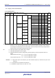
INTP0 to INTP5 input high-
level width, low-level width
t
INTH, tINTL 1
μ
s
KR0 to KR9 input available
width
t
KR 250 ns
RESET low-level width tRSL 10
μ
s
Remark fMCK: Timer array unit operation clock frequency
(Operation clock to be set by the timer clock select register 0 (TPS0) and the CKS0n bit of timer mode
register 0n (TMR0n). n: Channel number (n = 0 to 7))
<R>